Method for forming insulation film

a technology of insulating film and insulating film layer, which is applied in the direction of electrical control, machines/engines, transportation and packaging, etc., can solve the problems of increasing exponentially the leakage current due to a direct tunnel by quantum effect, the thickness reduction of gate insulating film has approached to its limit, and the leakage current can be easily formed, so as to reduce the thickness of the insulating film, the effect of reducing the thickness of the film

Inactive Publication Date: 2005-07-28
TOKYO ELECTRON LTD
View PDF9 Cites 296 Cited by
  • Summary
  • Abstract
  • Description
  • Claims
  • Application Information

AI Technical Summary

Benefits of technology

[0011] Another object of the present invention is to provide a process for forming a thin insulating film on the surface of a substrate for an electronic device, which can suitably carry out post-treatment (for example, formation of films by CVD or the like and etching) and can provide an insulating film excellent in both film quality and film thickness.
[0012] A further object of the present invention is to carry out various steps involved in the formation of an insulating film under the same principle of operation, thereby simplifying the apparatus form and efficiently forming an insulating film having an excellent characteristic.
[0013] As a result of earnest study, the present inventors have found that the formation of an insulating film by a method which enables not only the practice of one step in one apparatus as in the prior art but also the practice of various steps in a single apparatus is very effective for attaining the above objects.
[0015] For example, the present invention may include some embodiments wherein the application of plasma to a substrate for an electronic device using a process gas comprising at least a rare gas can provide a cleaning effect, the incorporation of oxygen or nitrogen in the same plasma causes oxidation or nitridation, or the application of the same plasma containing at least hydrogen to an oxygen atom-containing insulating film including an oxide film can reduce the thickness of the insulating film.
[0016] In the process for forming an insulating film according to the present invention having the above constitution, for example, an insulating film having any desired thickness can easily be formed by forming a film having a desired thickness with attention focused on film quality and then reducing the film thickness by a specific plasma treatment.

Problems solved by technology

The reason for this is that, in recent microfabricated, highly integrated and / or higher-performance devices, even a low level of leakage current may possibly cause severe problems, although such a leakage current does not pose substantially no problem in the case of conventional relatively low-integrated devices.
Typically, for example, in the development of a next-generation or advanced MOS transistor, with the advancement of the above microfabrication technique, the possible thickness reduction of gate insulating films has approached to its limit, and, consequently, a severe problem to be overcome has appeared.
However, when the film thickness is reduced to 2 nm or less, the leakage current due to a direct tunnel by quantum effect is increased exponentially, so as to increased the power consumption disadvantageously.
Typically, for example, in the development of next-generation MOS transistors, enhancing the level of microfabrication of high-performance silicon LSI poses problems of increased leakage current and increased power consumption.
However, the formation of a good-quality and thin insulating film is very difficult.
For example, an insulating film formed by conventional thermal oxidation or CVD (chemical vapor deposition method) is unsatisfactory in any one of characteristics, i.e., either film quality or film thickness.

Method used


Image

  • Method for forming insulation film
  • Method for forming insulation film
  • Method for forming insulation film

Examples


embodiment of

(One Embodiment of Production Process)

[0075] A process for forming of the above silicon oxynitride film will be described.

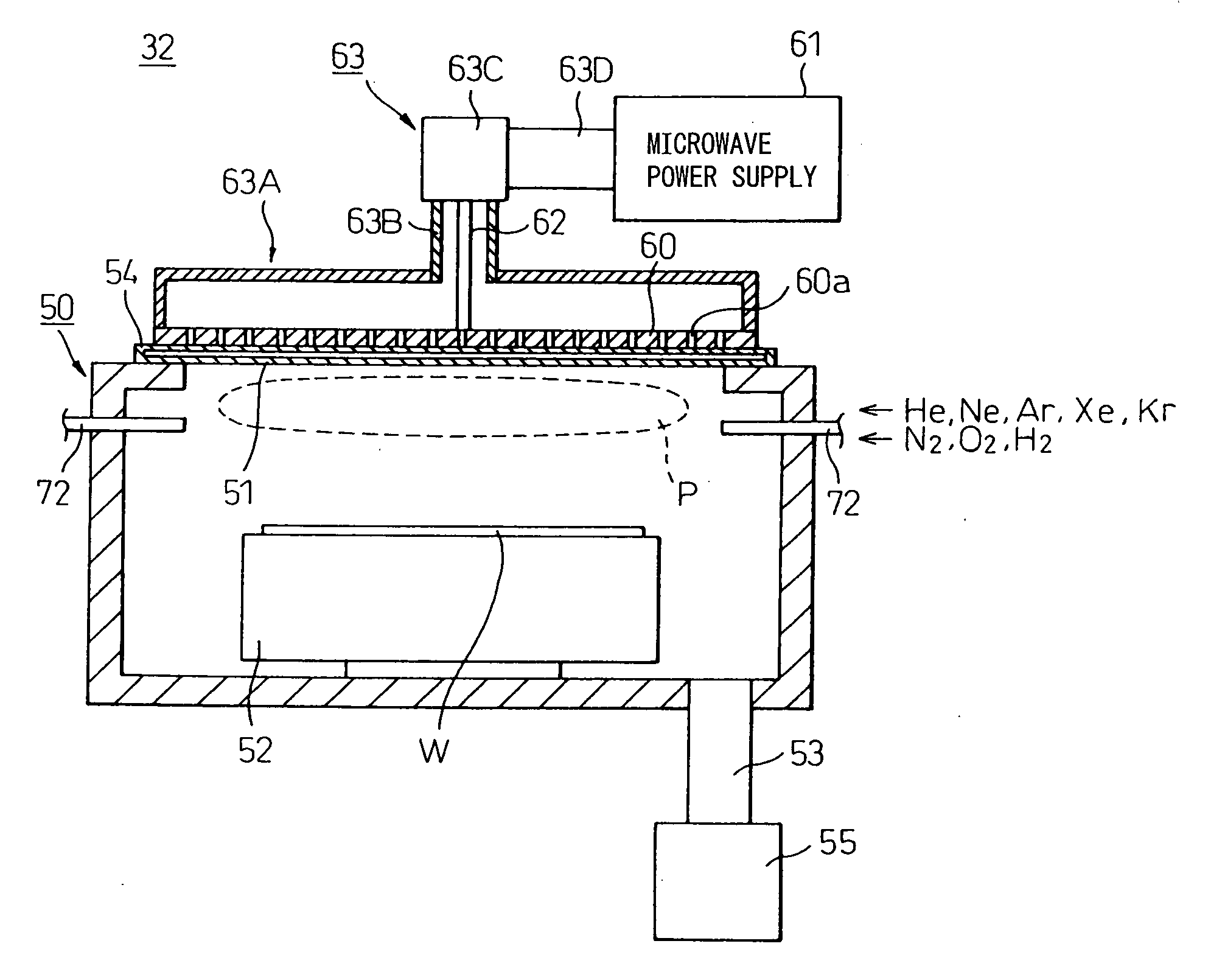
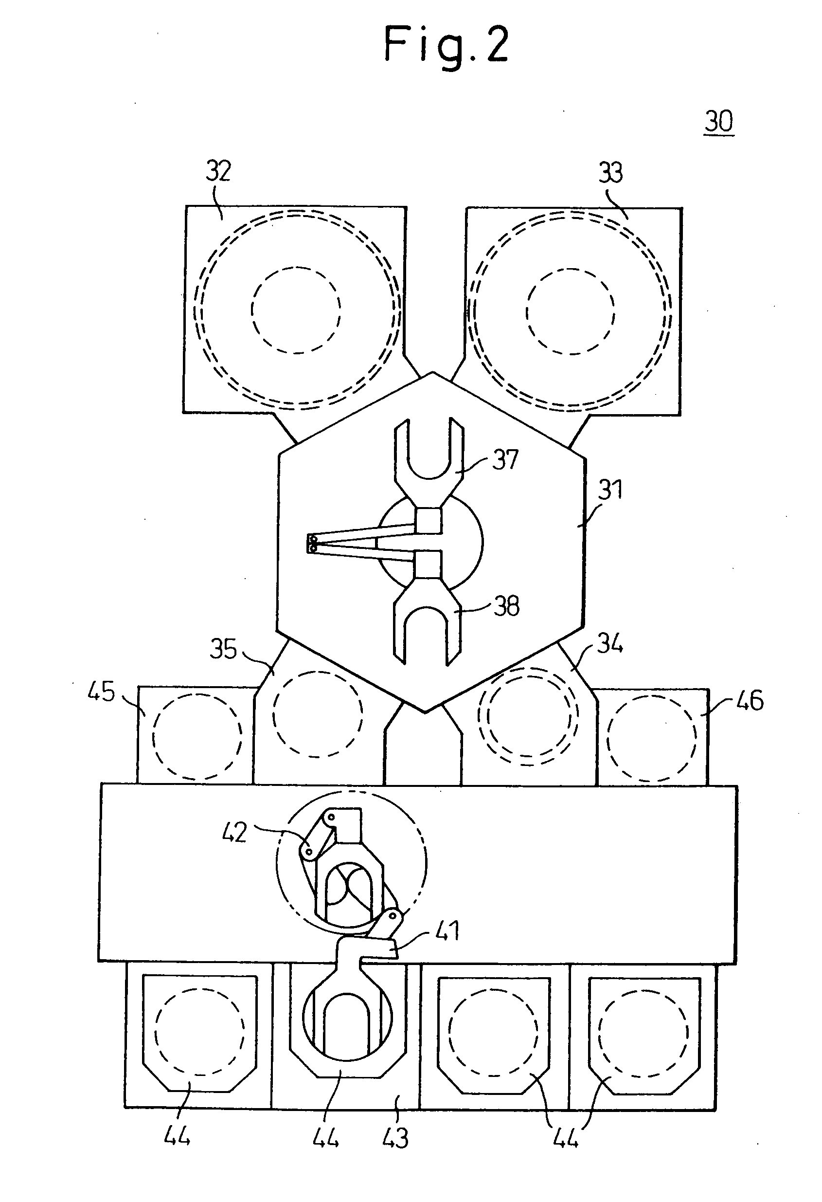
[0076]FIG. 2 is schematic view (schematic plan view) showing an example of the total arrangement of a semiconductor manufacturing equipment 30 for conducting the process for producing an electronic device material according to the present invention.

[0077] As shown in FIG. 2, in a substantially central portion of the semiconductor manufacturing equipment 30, there is disposed a transportation chamber 31 for transporting a wafer W (FIG. 3). Around the transportation chamber 31, there are disposed: plasma processing units 32 and 33 for conducting various treatments on the wafer, two load lock units 34 and 35 for conducting the communication / cutoff between the respective processing chambers, a heating unit 36 for operating various heating treatments, and a heating reaction furnace 47 for conducting various heating treatments on the wafer. These units are disposed s...

embodiment

(Embodiment of Plasma Processing)

[0091] Next, there is described an embodiment of the process processing to be used in the present invention.

[0092] A gate valve (not shown) provided at the side wall of the vacuum container 50 in the plasma processing unit 32 (FIG. 2) is opened, and the above-mentioned wafer W comprising the silicon substrate 1, and the field oxide film 11 formed on the surface of the silicon substrate 1 is placed on the stage 52 (FIG. 3) by means of transportation arms 37 and 38.

[0093] Next, the gate valve was closed so as to seal the inside of the vacuum container 50, and then the inner atmosphere therein is exhausted by the vacuum pump 55 through the exhaust pipe 53 so as to evacuate the vacuum container 50 to a predetermined degree of vacuum and a predetermined pressure in the container 50 is maintained. On the other hand, microwave (e.g., of 1.80 GHz and 2200 W) is generated by the microwave power supply 61, and the microwave is guided by the waveguide so that...

example 1

[0097] A device (N-type MOS capacitor) for carrying out various evaluations was formed by the following method.

[0098] (1): Substrate (FIG. 9)

[0099] As shown in FIG. 9, a P-type silicon substrate having a specific resistance of 8 to 12 Ωcm and plane orientation (100) was used as a substrate. The surface of the silicon substrate had a sacrificial oxide film with a thickness of 500 A (angstrom) previously formed by thermal oxidation.

[0100] (2): Cleaning Before Gate Oxidation

[0101] The sacrificial oxide film and contamination elements (metals and organic matter, particles) were removed by RCA cleaning using a combination of APM (a mixed liquid composed of ammonia, aqueous hydrogen peroxide, and pure water) with HPM (a mixed liquid composed of hydrochloric acid, aqueous hydrogen peroxide, and pure water) and DHF (a mixed liquid composed of hydrofluoric acid and pure water).

[0102] (3): Plasma Treatment Before Oxidation (FIG. 10)

[0103] After the treatment in the above step (2), RLSA ...


PUM

PropertyMeasurementUnit
thicknessaaaaaaaaaa
gate voltageaaaaaaaaaa
temperatureaaaaaaaaaa

Abstract

In a process involving the formation of an insulating film on a substrate for an electronic device, the insulating film is formed on the substrate surface by carrying out two or more steps for regulating the characteristic of the insulating film involved in the process under the same operation principle. The formation of an insulating film having a high level of cleanness can be realized by carrying out treatment such as cleaning, oxidation, nitriding, and a film thickness reduction while avoiding exposure to the air. Further, carrying out various steps regarding the formation of an insulating film under the same operation principle can realize simplification of the form of an apparatus and can form an insulating film having excellent property with a high efficiency.

Description

TECHNICAL FIELD [0001] The present invention relates to a process for forming an insulating film having various excellent characteristics (for example, control of very small film thickness and a high level of cleanness) with a high efficiency (for example, small footprint provided by conducting various steps in a single reaction chamber, or simplification of operationality and prevention of cross-contamination between apparatuses realized by conducting various steps in separate reaction chambers under the same principle of operation). The process for forming an electronic device material according to the present invention is suitably usable for the formation of a material, for example, for a semiconductor or a semiconductor device (for example, one having an MOS-type semiconductor structure with a gate insulating film having an excellent characteristic). BACKGROUND ART [0002] The present invention is generally and widely applicable to the formation of electronic device materials, fo...

Claims


Application Information

Patent Timeline
Patent Type & Authority Applications(United States)
IPC IPC(8): F02D41/02H01L21/3105H01L21/316H01L21/318H01L29/78
CPCH01L21/3105H01L21/3165Y10T428/12736Y10T428/12806H01L21/3185H01L21/0214H01L21/02164H01L21/02326H01L21/022H01L21/02329H01L21/0234
Inventor SUGAWARA, TAKUYATADA, YOSHIHIDENAKAMURA, GENJIOZAKI, SHIGENORINAKANISHI, TOSHIOSASAKI, MASARUMATSUYAMA, SEIJI
Owner TOKYO ELECTRON LTD
Why Eureka
Try Eureka