Single-crystal silicon substrate, SOI substrate, semiconductor device, display device, and manufacturing method of semiconductor device

a semiconductor device and single-crystal technology, applied in the direction of semiconductor devices, electrical devices, transistors, etc., can solve the problems of low heat resistance, hinder the improvement of productivity, and the performance of the transistor to form a high-performance silicon device, so as to achieve easy formation and enhance adhesive strength

Inactive Publication Date: 2009-03-24
SHARP KK
View PDF52 Cites 287 Cited by
  • Summary
  • Abstract
  • Description
  • Claims
  • Application Information

AI Technical Summary

Benefits of technology

[0035]To solve the above-described problem, the objective of the present invention is to provide (i) a semiconductor device in which a single-crystal silicon thin-film device can be easily formed on an insulating substrate without using an adhesive, a non-single-crystal silicon thin film and a single-crystal silicon thin-film device are formed, and high-performance systems are integrated, (ii) a method of manufacturing the semiconductor device, and (iii) a single-crystal silicon substrate for forming the single-crystal silicon thin film of the semiconductor device. Another objective of the present invention is to provide a method of manufacturing an SOI substrate in which an adhesive strength is enhanced, a display device, and a semiconductor device.

Problems solved by technology

This is because, when adopting P-Si, the mobility is decreased and an S (subthreshold) factor is increased due to localized states in a gap caused by the incompleteness of crystallinity and the deficiency around a grain boundary, so that the transistor does not have sufficient performance to form a high-performance silicon device.
However, according to this conventional semiconductor device and the manufacturing method thereof, since the adhesive is used for bonding the single-crystal silicon thin-film transistor, which has high performance, with the glass substrate, the bonding operation is cumbersome and hinders the improvement of productivity.
Further, being bonded using the adhesive, the semiconductor device has low heat resistance, and it is not possible to form high-quality members such as an inorganic insulating film and a TFT in the subsequent process.
For this reason, on the occasion of manufacturing an active matrix substrate, it is necessary to form a device including a TFT array before bonding the device to a substrate, and this has been a great disadvantage in terms of a cost / size ratio and formation of a wiring.
Moreover, WO93 / 15589 only teaches that a single-crystal silicon thin film device is formed on a glass substrate, and according to this arrangement, it is not possible to manufacture a high-performance / high-quality semiconductor device which has been sought after.
However, with this arrangement, it is not possible to increase resolution due to long wavelength of the light, and hence high-precision aligning cannot be performed.
However, it is not possible to obtain the required high performance when a conventionally-used amorphous silicon film or a polycrystal film is adopted.
Further, due to the increase of a subthreshold (S) factor, the performance of the transistor is caused to be insufficient so that a high-performance silicon device cannot be formed.
Moreover, when the crystallinity of the silicon film is insufficient, a fixed charge tends to be formed at the interface between silicon and a gate insulating film.
On this account, it is difficult to control a threshold voltage of the thin-film transistor, thereby being impossible to obtain a required threshold voltage.
In this process, since the energy of the laser causes a certain degree of fluctuation, the particle size of the obtained polycrystalline silicon film is not consistent.
In this process, since oxygen, which is a relatively heavy element, is implanted to a predetermined depth, a crystalline structure of the silicon wafer is seriously damaged due to an accelerating voltage involved in the implantation.
Thus, the SIMOX substrate has such a problem that the characteristics of single-crystal on the substrate are not sufficient.
Further, the insulation performance is inadequate due to non-stoichiometry of a silicon dioxide film layer, and since a large amount of oxygen is required for the implantation, the costs for the ion implantation is high.
However, in this arrangement, micro-roughness of the oxidized silicon film on the substrate weakens the adhesive power so that film stripping occurs.
Thus, the irregularity of the surface becomes noticeable and the adhesiveness of the bonding and the characteristics of the SOI substrate deteriorate.
However, the document does not mention the problems such as the formation of voids on the occasion of bonding and the stripping of the silicon film on the occasion of separation and stripping.
Further, Japanese Laid-Open Patent Application No. 6-268183 / 1994 does not describe the micro-roughness and flatness of the thinned semiconductor layer and the supporting substrate.
In this manner, the micro-roughness of the oxidized silicon film by which a light-transmitting substrate is covered weakens the adhesive power.

Method used


Image

  • Single-crystal silicon substrate, SOI substrate, semiconductor device, display device, and manufacturing method of semiconductor device
  • Single-crystal silicon substrate, SOI substrate, semiconductor device, display device, and manufacturing method of semiconductor device
  • Single-crystal silicon substrate, SOI substrate, semiconductor device, display device, and manufacturing method of semiconductor device

Examples


first embodiment

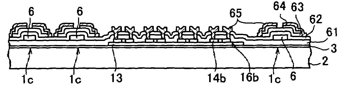
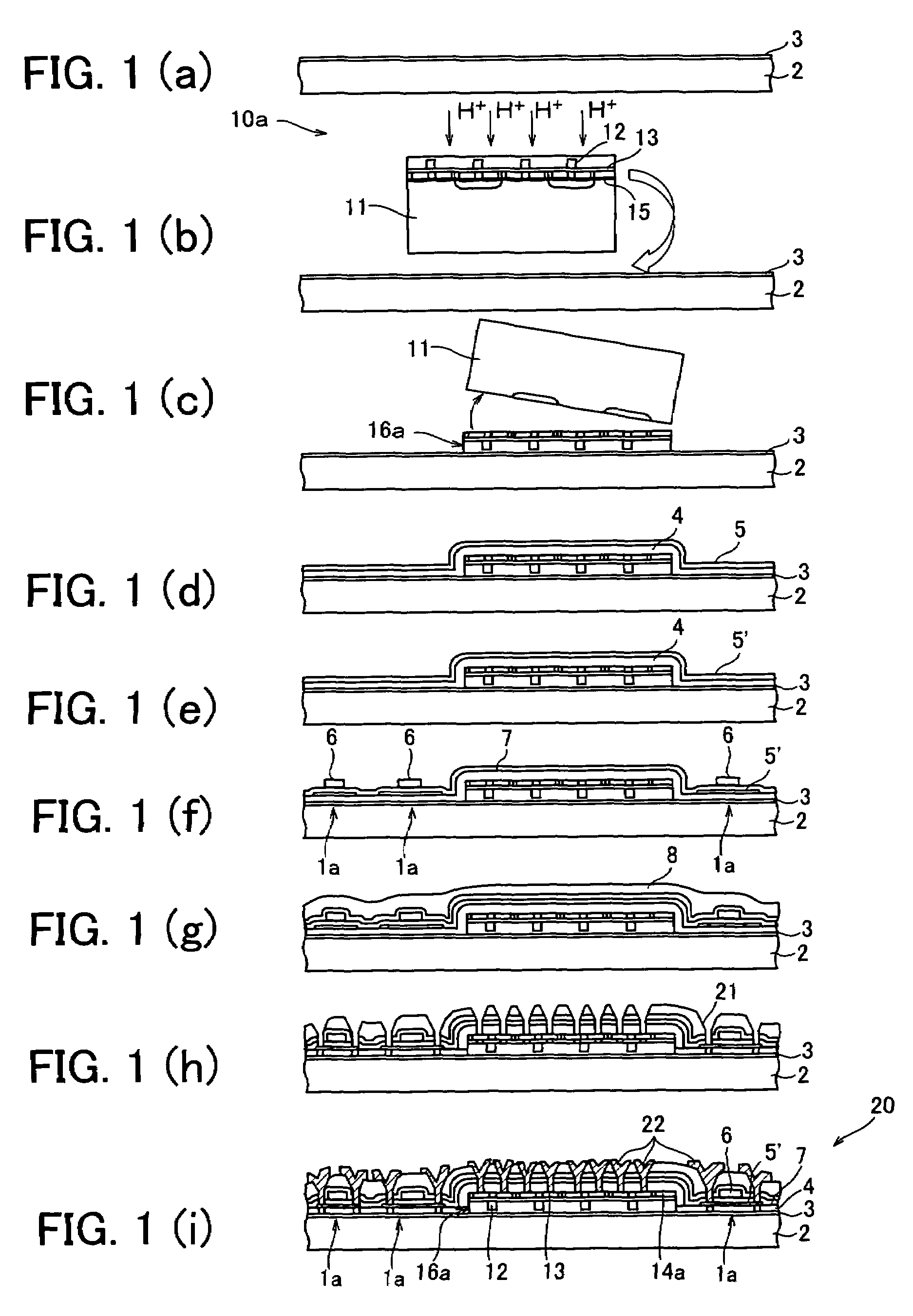
[0140]The following will describe a single-crystal silicon substrate, a semiconductor device, and a manufacturing method thereof in accordance with an embodiment of the present invention. FIGS. 1(a)-1(i) are cross sections illustrating a manufacturing process of a semiconductor device of the present embodiment. The semiconductor device of the present embodiment is a high-performance and highly-functional semiconductor device in which a MOS non-single-crystal silicon thin-film transistor and a MOS single-crystal silicon thin-film transistor are formed on different areas of the surface of an insulating substrate, the semiconductor device being formed on a TFT active matrix substrate.

[0141]The MOS thin-film transistor includes an active semiconductor layer, gate electrodes, a gate insulating film, and high-concentration impurity doped sections (source and drain electrodes) formed on the both sides of the gate. The MOS thin-film transistor is a typical transistor in which the gate elect...

embodiment 2

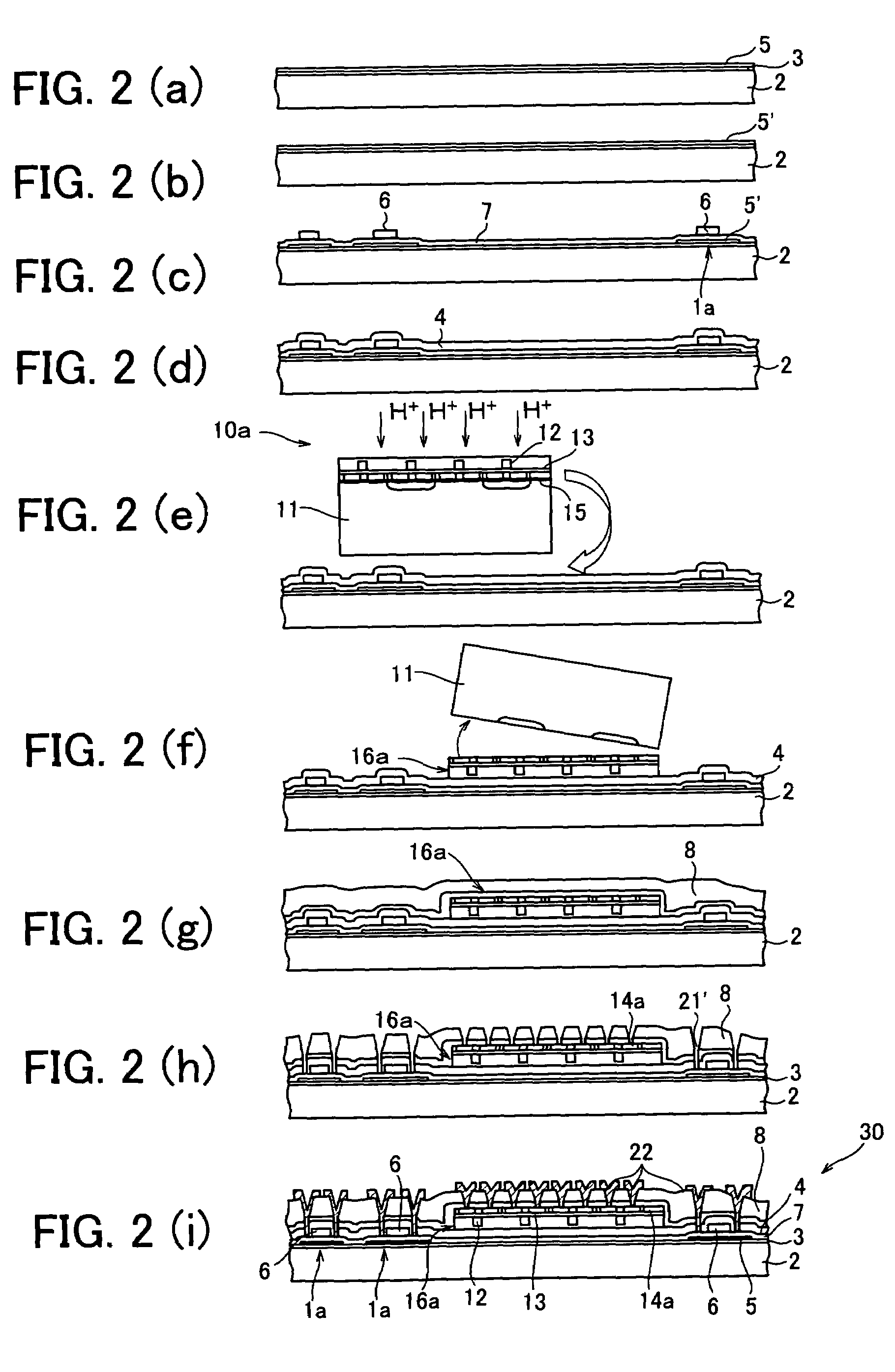
[0191]The following will describe another embodiment of a single-crystal silicon substrate, a semiconductor device, and a method of manufacturing the same, in accordance with the present invention. FIGS. 2(a)-2(i) are cross sections illustrating a manufacturing process of the semiconductor device of said another embodiment of the present invention. By the way, members having the same functions as those described in Embodiment 1 are given the same numbers, so that the descriptions are omitted for the sake of convenience.

[0192]Being identical with the above-described semiconductor device 20 of Embodiment 1, a semiconductor device 30 of the present embodiment is arranged in such a manner that, a MOS single-crystal silicon thin-film transistor 16a and a non-single-crystal silicon thin-film transistor 1a are formed in different areas of an insulating substrate 2. Thus, the semiconductor device 30 of the present embodiment is also high-performance and highly functional, as the semiconduct...

embodiment 3

[0215]The following will describe a further embodiment of a single-crystal silicon substrate, a semiconductor device, and a method of manufacturing the same, in accordance with the present invention. FIGS. 3(a)-3(f) are cross sections illustrating a manufacturing process of the semiconductor device of the present embodiment. By the way, members having the same functions as those described in Embodiments 1 and 2 are given the same numbers, so that the descriptions are omitted for the sake of convenience.

[0216]As is the case with Embodiment 1, a semiconductor device 40 of the present embodiment is, as shown in FIG. 3(f), arranged such that a non-single-crystal silicon thin-film transistor and a single-crystal silicon thin-film transistor are formed on a single insulating substrate 2. While the present embodiment is identical with Embodiment 1 to the extent that the single-crystal silicon thin-film transistor is formed before the formation of the non-single-crystal silicon thin-film tr...


PUM

PropertyMeasurementUnit
thicknessaaaaaaaaaa
thicknessaaaaaaaaaa
thicknessaaaaaaaaaa

Abstract

A semiconductor device of the present invention is arranged in such a manner that a MOS non-single-crystal silicon thin-film transistor including a non-single-crystal silicon thin film made of polycrystalline silicon, a MOS single-crystal silicon thin-film transistor including a single-crystal silicon thin film, and a metal wiring are provided on an insulating substrate. With this arrangement, (i) a semiconductor device in which a non-single-crystal silicon thin film and a single-crystal silicon thin-film device are formed and high-performance systems are integrated, (ii) a method of manufacturing the semiconductor device, and (iii) a single-crystal silicon substrate for forming the single-crystal silicon thin-film device of the semiconductor device are obtained.

Description

FIELD OF THE INVENTION[0001]The present invention relates to a semiconductor device for improving circuit performances of devices such as an active matrix liquid crystal display device driven by TFT, in which a peripheral drive circuit and a control circuit are integrated on a single substrate, a manufacturing method of the semiconductor device, and a single-crystal silicon substrate used in the process of manufacturing the semiconductor device. Further, the present invention relates to an SOI (Silicon On Insulator) substrate, a display device, and a manufacturing method of a semiconductor device, and particularly relates to (i) an SOI substrate including a single-crystal silicon thin film which is obtained by bonding a single-crystal silicon piece, to which hydrogen ions are implanted, with a substrate, and dividing the substrate with the single-crystal silicon piece at a layer to which the hydrogen ions are implanted, (ii) a display device using the SOI substrate, and (iii) a meth...

Claims


Application Information

Patent Timeline
Patent Type & Authority Patents(United States)
IPC IPC(8): H01L21/00H01L21/762H01L21/77H01L21/84H01L27/12H01L27/32H01L29/786
CPCH01L21/76254H01L27/1229H01L27/1251H01L27/1266H01L29/78603H01L29/78654H01L2924/1305H01L2924/12032H01L2924/13091H01L21/26506H01L2924/12041H01L27/3244H01L29/78666H01L29/78675H01L2221/68363H01L2224/24226H01L2924/01046H01L2924/01057H01L2924/01078H01L2924/01079H01L2924/01019H01L2924/01021H01L2924/00H01L2924/12044H01L21/26566H01L21/2658H10K59/12
Inventor TAKAFUJI, YUTAKAITOGA, TAKASHI
Owner SHARP KK
Why Eureka
Try Eureka