
Light-Emitting Device and Method for Manufacturing the Same

a technology of light-emitting devices and manufacturing methods, which is applied in the direction of thermoelectric device junction materials, semiconductor devices, electrical apparatus, etc., can solve the problems of reducing the external electroluminescence quantum efficiency, reducing the luminescence or brightness in directions extending outwardly from the surface of the device, and reducing the planarizing effect of the planarizing layer

Inactive Publication Date: 2013-08-15
NEDERLANDSE ORG VOOR TOEGEPAST-NATUURWETENSCHAPPELIJK ONDERZOEK (TNO) +1
View PDF9 Cites 20 Cited by
  • Summary
  • Abstract
  • Description
  • Claims
  • Application Information

AI Technical Summary

Benefits of technology

The patent discusses the use of a light extraction layer in OLED devices. The layer with micro-lens portions aims to improve light output efficiency, but a conflicting patent describes a different layer that causes blurring. The text describes a method for obtaining an organic layer with dispersed domains of two mutually immiscible substances, which can control the average size of the domains and optical properties. The dispersion can be applied in liquid form, which makes it easier to planarize and manufacture. The technical effects of the patent text includes improving light output efficiency and controlling optical properties in OLED devices.

Problems solved by technology

These phenomena result in decreased external electroluminescence quantum efficiency and a reduction in the luminescence or brightness in directions extending outwardly from the surface of the device.
The presence of the microparticles reduces the planarizing effect of the planarizing layer.

Method used


Image

  • Light-Emitting Device and Method for Manufacturing the Same
  • Light-Emitting Device and Method for Manufacturing the Same
  • Light-Emitting Device and Method for Manufacturing the Same

Examples


Embodiment Construction

[0039]In the following detailed description numerous specific details are set forth in order to provide a thorough understanding of the present invention. However, it will be understood by one skilled in the art that the present invention may be practiced without these specific details. In other instances, well known methods, procedures, and components have not been described in detail so as not to obscure aspects of the present invention.

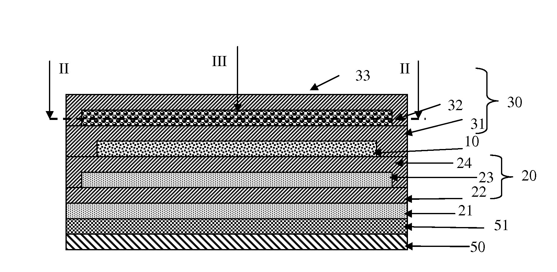
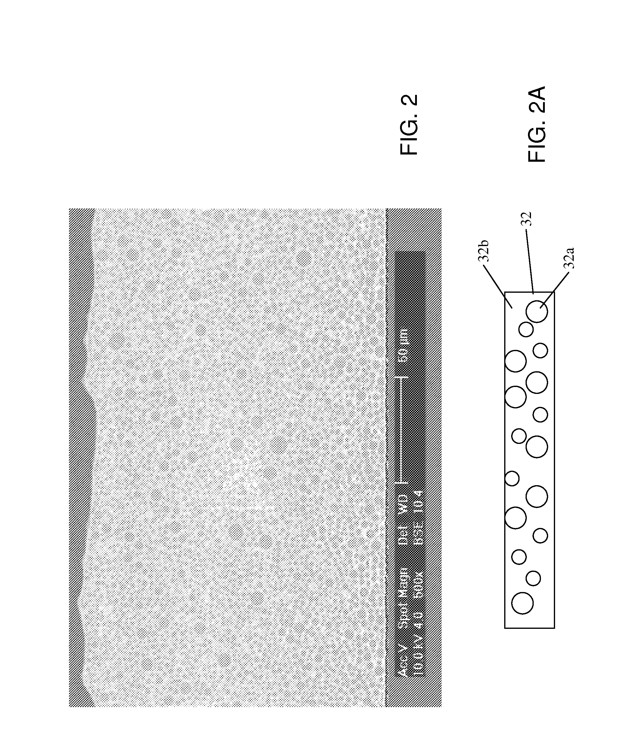
[0040]The invention is described more fully hereinafter with reference to the accompanying drawings, in which embodiments of the invention are shown. This invention may, however, be embodied in many different forms and should not be construed as limited to the embodiments set forth herein. Rather, these embodiments are provided so that this disclosure will be thorough and complete, and will fully convey the scope of the invention to those skilled in the art. In the drawings, the size and relative sizes of layers and regions may be exaggerated for c...


PUM


Abstract

A light-emitting device is disclosed comprising an organic light-emitting diode structure and an encapsulation comprising a light-transmitting window with at least a first inorganic layer, an organic layer and a second inorganic layer, the organic layer comprising domains of a dispersed first organic component embedded by a second component, the first and the second component having a mutually different refractive index, the organic layer being sandwiched between the first and the second inorganic layer.

Description

BACKGROUND OF THE INVENTION[0001]1. Field of the invention[0002]The present invention relates to a light-emitting device. The present invention further relates to a method for manufacturing a light-emitting device.[0003]2. Related Art[0004]Organic light emitting devices (“OLEDs”), including both polymer and small-molecule OLEDs, are potential candidates for a great variety of virtual- and direct-view type displays, such as lap-top computers, televisions, digital watches, telephones, pagers, cellular telephones, calculators and the like. Unlike inorganic semiconductor light emitting devices, organic light emitting devices are generally simple and are relatively easy and inexpensive to fabricate. Also, OLEDs readily lend themselves to applications requiring a wide variety of colors and to applications that concern large-area devices.[0005]OLEDs generate light when an electron and a hole combine in a light-emitting layer in the OLED to generate a photon. The percentage of combined elec...

Claims


Application Information

Patent Timeline
Patent Type & Authority Applications(United States)
IPC IPC(8): H01L51/52
CPCH01L51/5237H01L51/5246H01L51/5253H01L51/5275H10K50/8445H10K50/858H01L2924/06H01L2924/0635H10K85/10H10K50/84H10K50/844H10K50/8426
Inventor YOUNG, EDWARD WILLEM ALBERTWILSON, JOANNE SARAHHARKEMA, STEPHANHERMES, DOROTHEE CHRISTINEMICHELS, JASPER JOOSTVAN MOL, ANTONIUS MARIA BERNARDUSGALAND, EMILIEFRANTZ, RICHARDKOTZEV, DIMITER LUBOMIROV
Owner NEDERLANDSE ORG VOOR TOEGEPAST-NATUURWETENSCHAPPELIJK ONDERZOEK (TNO)
Learn More