Method for preventing electric charge generation in high voltage device manufacturing process

A process and high-voltage device technology, which is applied in semiconductor/solid-state device manufacturing, circuits, electrical components, etc., can solve the problems of large leakage of isolation structure, low device opening voltage, and inability to isolate, so as to improve stability and stability High, the effect of normal device characteristics

Active Publication Date: 2010-08-11
SHANGHAI HUAHONG GRACE SEMICON MFG CORP
View PDF0 Cites 0 Cited by
  • Summary
  • Abstract
  • Description
  • Claims
  • Application Information

AI Technical Summary

Problems solved by technology

The consequence is that the turn-on voltage of the device is too low, and even cause depletion
In addition, the leakage of the isolation structure is very large (10 -6 A), so that it cannot play an effective isolation role
[0005] Existing N 2 , H 2 Annealing method is difficult to eliminate the impact of charge on high voltage devices

Method used


Image

  • Method for preventing electric charge generation in high voltage device manufacturing process
  • Method for preventing electric charge generation in high voltage device manufacturing process
  • Method for preventing electric charge generation in high voltage device manufacturing process

Examples


Embodiment Construction

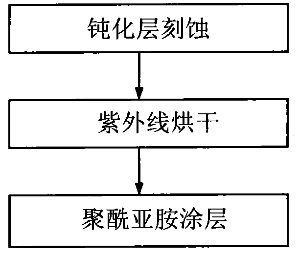
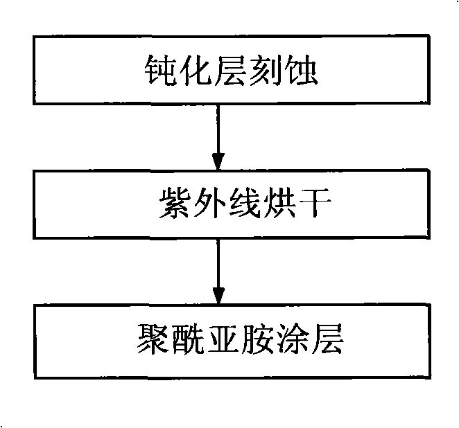
[0014] Aiming at the impact of charges on high-voltage devices, the present invention adopts the method of ultraviolet drying to release charges, that is, to use ultraviolet light energy to recombine the charges generated in various manufacturing processes (the energy of ultraviolet rays can neutralize the charges generated in the oxide layer). A large number of electron-hole pairs), so as to achieve the effect of releasing charges.

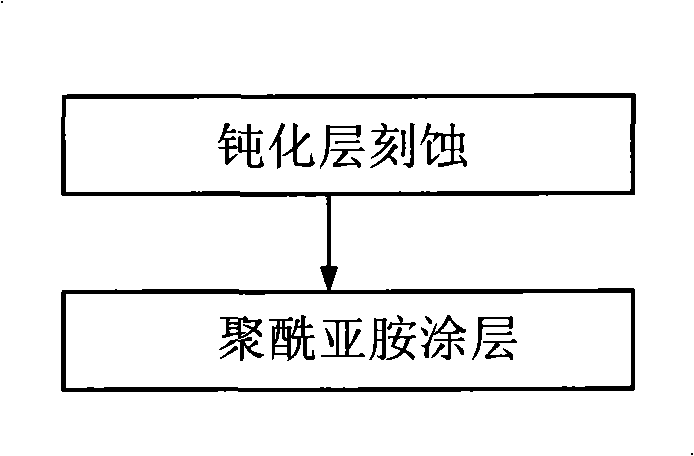
[0015] Referring to Figures 1 and 2, the ultraviolet drying described in the present invention needs to be carried out after the subsequent metal connection and passivation layer etching, especially after the passivation layer is etched. Then followed by polyimide coating process. In the existing process, the polyimide coating process is directly performed after the passivation layer is etched.

[0016] When the method of the present invention is used for specific implementation, it is necessary to select an ultraviolet drying device, time and t...


PUM


Abstract

The invention discloses a method for preventing the generation of charges in the technological processing procedure of a high-voltage device, which comprises the following steps: performing ultraviolet ray drying first after the finishing a step of etching a passivation layer; and performing a processing step of a polyimide coating. The method can eliminate the influence on the high-voltage device caused by the charges.

Description

[0001] The present invention is a divisional application of the invention patent application with the application number: 200610117167.1, the application date: October 16, 2006, and the invention title: "Method for preventing charge generation in the process of high-voltage devices". technical field [0002] The invention relates to a manufacturing process method of a semiconductor integrated circuit, in particular to a method for preventing charge generation in the process process of a high-voltage device. Background technique [0003] In today's high-voltage devices, there will be a well with a very light concentration, so the concentration on the channel surface will also be very light. If a large amount of charge is generated during the process, it will cause a lot of mobile electrons to be generated on the surface of the high-voltage device, which will cause excessive leakage of the device and seriously cause the device to fail. [0004] The reason for the charge genera...

Claims


Application Information

Patent Timeline
Patent Type & Authority Patents(China)
IPC IPC(8): H01L21/00H01L21/268H01L21/3105H01L21/336
Inventor 陆涵蔚李健刘春玲
Owner SHANGHAI HUAHONG GRACE SEMICON MFG CORP
Why Eureka
Try Eureka