Processing equipment with good dustproof effect for semiconductor device manufacturing

A technology for processing equipment and semiconductors, which is applied in semiconductor/solid-state device manufacturing, electrical components, cleaning methods and appliances, etc., and can solve problems such as poor dustproof effect

A technology for processing equipment and semiconductors, which is applied in semiconductor/solid-state device manufacturing, electrical components, cleaning methods and appliances, etc., and can solve problems such as poor dustproof effect

CN112808699AInactive Publication Date: 2021-05-18泗阳垠创运营管理有限公司

Image

  • Processing equipment with good dustproof effect for semiconductor device manufacturing
  • Processing equipment with good dustproof effect for semiconductor device manufacturing
  • Processing equipment with good dustproof effect for semiconductor device manufacturing

Examples


Embodiment Construction

[0029] The following will clearly and completely describe the technical solutions in the embodiments of the present invention with reference to the accompanying drawings in the embodiments of the present invention. Obviously, the described embodiments are only some, not all, embodiments of the present invention. Based on the embodiments of the present invention, all other embodiments obtained by persons of ordinary skill in the art without making creative efforts belong to the protection scope of the present invention.

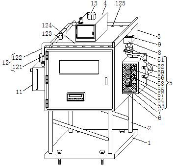
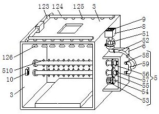
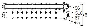
[0030] see Figure 1-8 , an embodiment provided by the present invention:

[0031]A kind of processing equipment for the manufacture of semiconductor devices with good dustproof effect, comprising a support plate 1, a support frame 2 is bolted to the front and back of the top of the support plate 1, a processing box 3 is bolted to the top of the support frame 2, and the processing box 3 The inner cavity of the processing box 3 is provided with a dust-proof me...


PUM


Abstract

The invention discloses processing equipment with good dustproof effect for semiconductor device manufacturing. The equipment comprises a supporting plate, supporting frames are bolted to the front surface and the back surface of the top of the supporting plate, a processing box is bolted to the tops of the supporting frames, a dustproof mechanism is arranged in an inner cavity of the processing box, and a dust collection mechanism matched with the dustproof mechanism for use is arranged at the top of the inner cavity of the processing box. According to the equipment, through cooperation of a first air pump, a hose, a second motor, a driving gear, a first driven gear, a second driven gear, fixing pipes, a connecting pipe, a U-shaped pipe and a nozzle, a user can conveniently use the second motor to drive the two groups of the fixing pipes to rotate at the same time, so that the inner cavity of the processing box is blown in all directions through the rotating nozzle, furthermore, dust in the processing box is always in a floating state, and through cooperation of a second air pump, a ventilation pipe, a flow dividing pipe, a diffusion pipe, a pipeline and suction heads, the user can conveniently use the second air pump to drive the multiple suction heads to rapidly absorb the floating dust.

Description

technical field [0001] The invention relates to the technical field of semiconductor devices, in particular to a processing equipment for manufacturing semiconductor devices with good dust-proof effect. Background technique [0002] A semiconductor device is an electronic device whose conductivity is between a good conductor and an insulator. It uses the special electrical characteristics of semiconductor materials to complete specific functions. It can be used to generate, control, receive, transform, amplify signals and perform energy conversion. The semiconductor of semiconductor devices The material is silicon, germanium or gallium arsenide, which can be used as rectifiers, oscillators, light emitters, amplifiers, photometers and other equipment. The basic structure of most two-terminal devices (ie, crystal diodes) is a PN junction. [0003] As the demand for semiconductor devices continues to increase, users need to use processing equipment to process semiconductor devi...

Claims


Application Information

Patent Timeline
18 May 2021
Publication
CN112808699A
IPC
B08B5/02; B08B5/04; B01D46/10; H01L21/67
CPC
B01D46/10; B08B5/02; B08B5/04; H01L21/67028
Inventors
金安年