Check patentability & draft patents in minutes with Patsnap Eureka AI!

Back drilling method of PCB, and PCB

A PCB board and back-drilling technology, which is applied in the PCB back-drilling method and the field of PCB boards, can solve the problems of difficulty in obtaining PCB boards accurately and high risk of residual copper, and achieve the effect of reducing hole deviation and risk of residual copper

Active Publication Date: 2021-05-28
SHENNAN CIRCUITS
View PDF4 Cites 0 Cited by
  • Summary
  • Abstract
  • Description
  • Claims
  • Application Information

AI Technical Summary

Problems solved by technology

[0004] This application provides a method for back-drilling PCB boards to solve the technical problem that it is difficult to accurately obtain the entry hole position for back-drilling PCB boards in the prior art, resulting in a high risk of residual copper

Method used


Image

  • Back drilling method of PCB, and PCB
  • Back drilling method of PCB, and PCB
  • Back drilling method of PCB, and PCB

Examples


Embodiment Construction

[0026] In order to make the technical problems solved by the present application, the technical solutions adopted and the technical effects achieved more clearly, the technical solutions of the embodiments of the present application will be further described in detail below with reference to the accompanying drawings.

[0027] Reference herein to an "embodiment" means that a particular feature, structure, or characteristic described in connection with the embodiment can be included in at least one embodiment of the present application. The appearances of the phrase in various places in the specification are not necessarily all referring to the same embodiment, nor a separate or alternative embodiment that is mutually exclusive of other embodiments. It is explicitly and implicitly understood by those skilled in the art that the embodiments described herein may be combined with other embodiments.

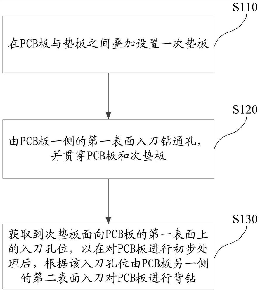
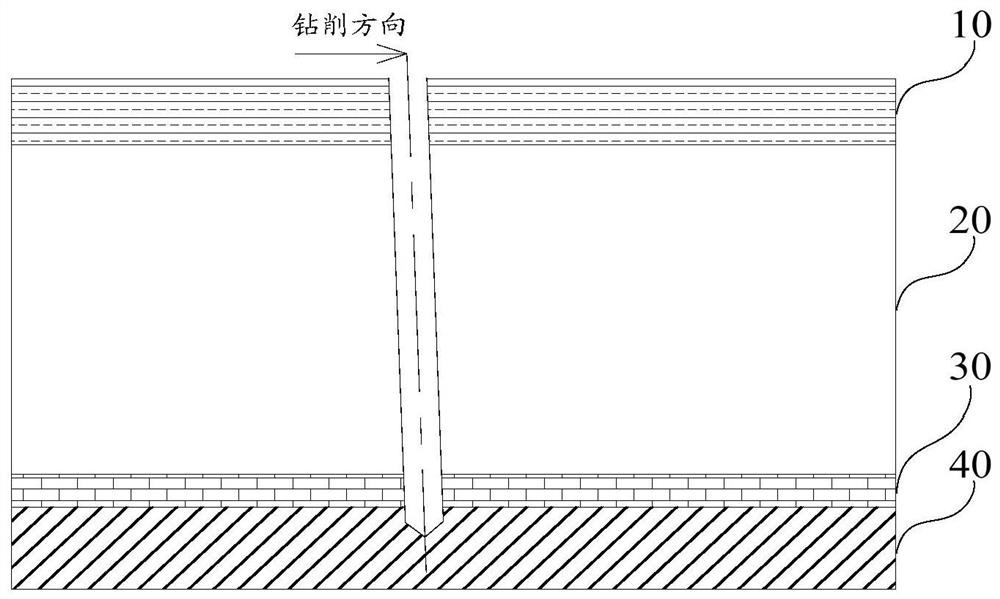
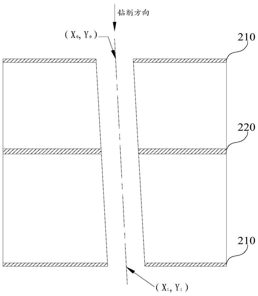
[0028] see Figures 1a-1e ,in, Figure 1a is the schematic flow chart of the fir...


PUM

PropertyMeasurementUnit
Thicknessaaaaaaaaaa

Abstract

The invention discloses a back drilling method of a PCB, and a PCB. The method comprises the steps: arranging a primary backing plate between the PCB and a backing plate in an overlapping manner; drilling a through hole from the first surface of one side of the PCB, and penetrating through the PCB and a secondary backing plate; and obtaining a tool entering hole position on the first surface, facing the PCB, of the secondary backing plate, so that after the PCB is subjected to primary treatment, tool entering is carried out on the PCB from the second surface of the other side of the PCB according to the tool entering hole position, and back drilling is carried out on the PCB. By means of the mode, when the through hole is drilled in the PCB, the primary backing plate is introduced once, the tool entering hole position during back drilling of the PCB is more accurately obtained through the backing plate, and therefore under the condition that the hole position precision of a remaining copper hole after back drilling is not lost, hole deviation of the through hole and a back drilling hole can be reduced, and the residual copper risk is reduced.

Description

technical field [0001] The present application relates to the technical field of PCB boards, and in particular, to a method for back drilling a PCB board and a PCB board. Background technique [0002] At present, as the server is advancing in the direction of high speed and integration, it puts forward higher requirements on the structure of the PCB board with high aspect ratio and high density on the server, and the back drilling process is controlled accordingly. One of the key processes of signal loss. [0003] Among them, the increase of the thickness-diameter ratio of the PCB board will cause a certain loss of hole position accuracy in the process of through-hole drilling, so that the back-drilling and the through-hole are deviated, and the risk of residual copper is increased. In addition, due to the deviation of the entry surface and the exit surface of the through hole, the light transmittance is weakened, and the difficulty of accurately obtaining the hole position...

Claims


Application Information

Patent Timeline
IPC IPC(8): H05K3/00
CPCH05K3/0047H05K2203/0214
Inventor 林淡填廖志强吴杰刘海龙杨中瑞余晋磊
Owner SHENNAN CIRCUITS
Features
  • R&D
  • Intellectual Property
  • Life Sciences
  • Materials
  • Tech Scout
  • Unparalleled Data Quality
  • Higher Quality Content
  • 60% Fewer Hallucinations
Learn More