Array substrate, display panel and display terminal

An array substrate and display panel technology, applied to static indicators, instruments, etc., can solve problems such as weak voltage stabilization capability, decreased aperture ratio, and unstable voltage of the common electrode layer, achieving stable voltage and reducing horizontal crosstalk

Pending Publication Date: 2022-01-28
HUIZHOU CHINA STAR OPTOELECTRONICS TECHNOLOGY CO LTD +1
View PDF4 Cites 0 Cited by
  • Summary
  • Abstract
  • Description
  • Claims
  • Application Information

AI Technical Summary

Problems solved by technology

[0004] An embodiment of the present invention provides an array substrate, which is used to solve the problem that the voltage instability of the common electrode layer of the array substrate in the prior art is likely to cause horizontal crosstalk on the display screen. If additional metal lines are used to connect, the aperture ratio will decrease. And technical problems with weak voltage stabilization ability

Method used


Image

  • Array substrate, display panel and display terminal
  • Array substrate, display panel and display terminal
  • Array substrate, display panel and display terminal

Examples


Embodiment Construction

[0022] The following will clearly and completely describe the technical solutions in the embodiments of the present invention with reference to the drawings in the embodiments of the present invention. In the drawings, for clarity and ease of understanding and description, the size and thickness of the components shown in the drawings are not in scale.

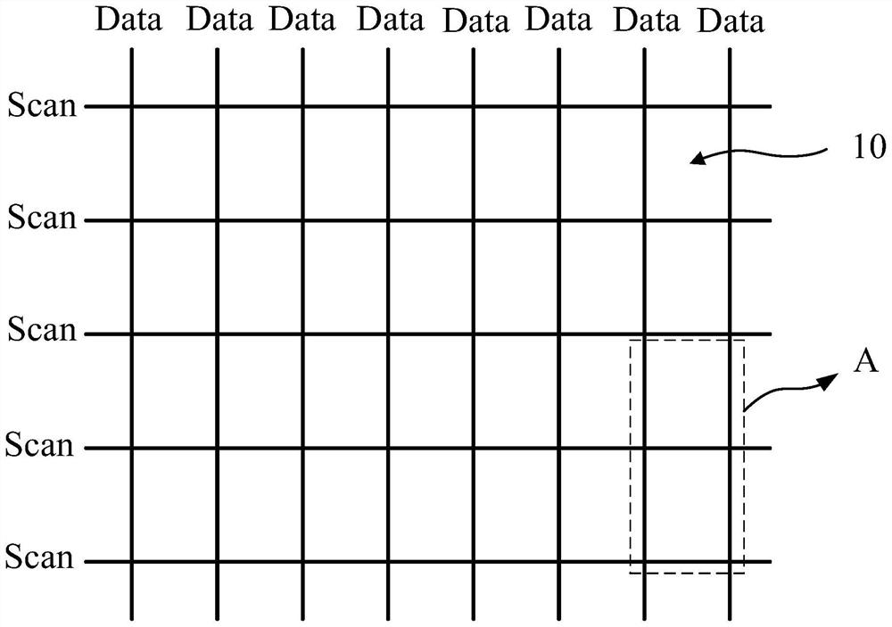
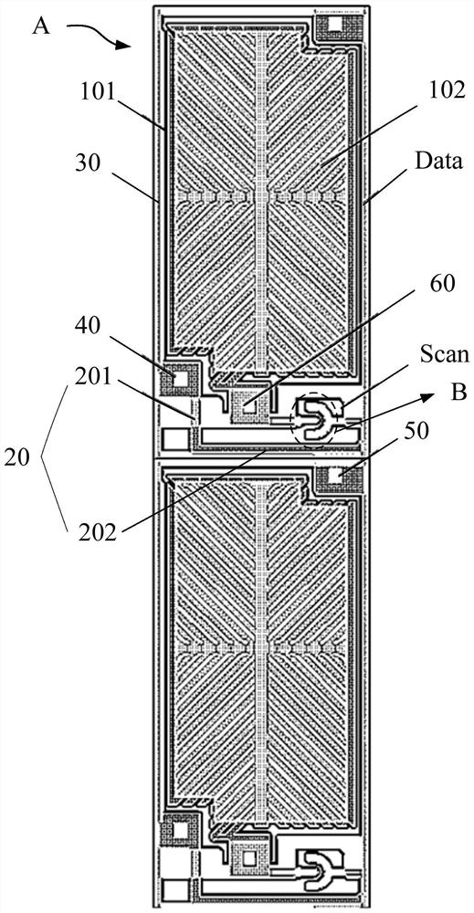
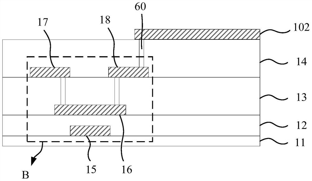
[0023] like figure 1 and figure 2 As shown in , are respectively the schematic diagram of the basic structure of the array substrate provided by the embodiment of the present invention and figure 1 In the enlarged view at A, the array substrate includes multiple scan lines Scan and multiple data lines Data intersecting the multiple scan lines Scan, the multiple scan lines Scan and the multiple data lines Data Surrounded by a plurality of pixel units 10; each of the pixel units 10 includes a common electrode layer 101; wherein, the array substrate also includes a shield connection line 20, in the extending direction of the d...


PUM


Abstract

The invention provides an array substrate, a display panel and a display terminal, the array substrate comprises a plurality of scanning lines and a plurality of data lines crossed with the scanning lines, and the scanning lines and the data lines define a plurality of pixel units; each pixel unit comprises a common electrode layer; the array substrate further comprises shielding connecting lines, and in the extending direction of the data lines, the public electrode layers in every two adjacent pixel units are electrically connected through the shielding connecting lines. The adjacent common electrode layers are electrically connected through the shielding connecting lines to form a common electrode layer cross-linked network, the voltage of the common electrode layers is equal to that of the shielding connecting lines, the voltage of the common electrode layers can be further stabilized, horizontal crosstalk can be reduced, additional metal lines are not needed, and the aperture opening ratio cannot be lost.

Description

technical field [0001] The present invention relates to the field of display technology, in particular to an array substrate, a display panel and a display terminal. Background technique [0002] Liquid Crystal Display (LCD) has many advantages such as thin body, power saving, and no radiation, and has been widely used, such as: LCD TV, mobile phone, personal digital assistant (PDA), digital camera, computer screen or Laptop screens, etc., dominate the field of flat panel displays. The liquid crystal display includes an array substrate, a color filter substrate, and a liquid crystal layer located between the array substrate and the color filter substrate. The array substrate is provided with multiple common electrode layers (Com), and the multiple common electrode layers do not form cross-linking in the plane. Network, the voltage of the common electrode layer is easily coupled by the Data (data line) signal, which is one of the direct causes of horizontal crosstalk in the ...

Claims


Application Information

Patent Timeline
Patent Type & Authority Applications(China)
IPC IPC(8): G09G3/36
CPCG09G3/36G09G2300/0426G09G2320/0209
Inventor 湛志明
Owner HUIZHOU CHINA STAR OPTOELECTRONICS TECHNOLOGY CO LTD
Why Eureka
Try Eureka