Adjusting device and semiconductor heat treatment equipment

A technology of heat treatment equipment and adjustment device, which is used in semiconductor/solid device manufacturing, coating, gaseous chemical plating, etc. Effect

Active Publication Date: 2022-07-12
BEIJING NAURA MICROELECTRONICS EQUIP CO LTD
View PDF6 Cites 0 Cited by
  • Summary
  • Abstract
  • Description
  • Claims
  • Application Information

AI Technical Summary

Problems solved by technology

[0006] The purpose of the embodiment of the present application is to provide an adjustment device and semiconductor heat treatment equipment, which can at least solve the problems that the apron fixing method cannot avoid interference and the holder is easy to damage the pipe

Method used


Image

  • Adjusting device and semiconductor heat treatment equipment
  • Adjusting device and semiconductor heat treatment equipment
  • Adjusting device and semiconductor heat treatment equipment

Examples


Embodiment Construction

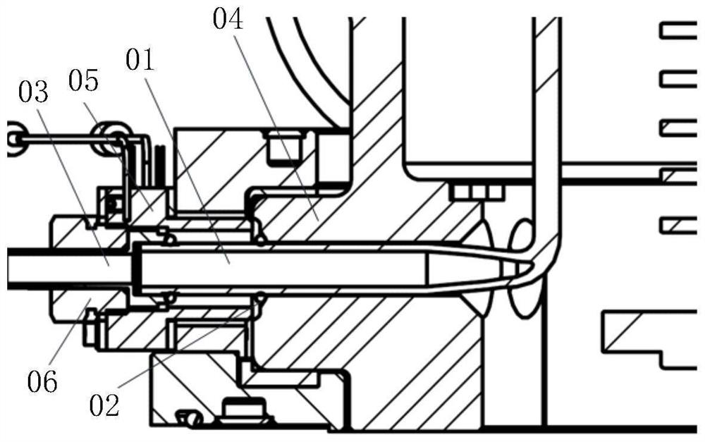
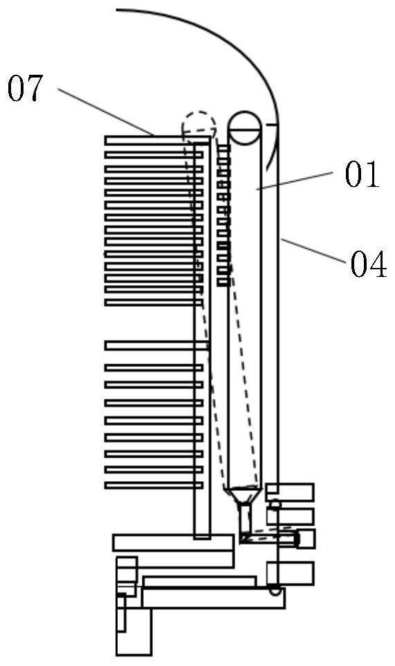
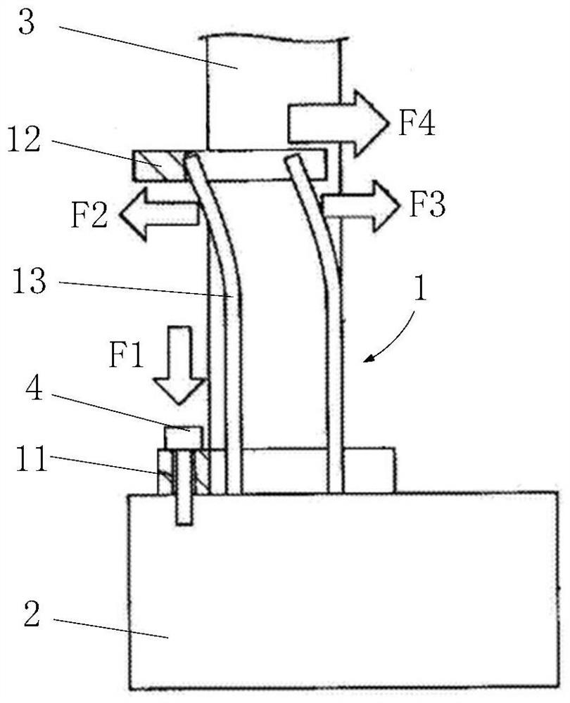
[0037] The technical solutions in the embodiments of the present application will be clearly and completely described below with reference to the accompanying drawings in the embodiments of the present application. Obviously, the described embodiments are part of the embodiments of the present application, not all of the embodiments. Based on the embodiments in this application, all other embodiments obtained by those of ordinary skill in the art without creative work fall within the protection scope of this application.

[0038] The terms "first", "second" and the like in the description and claims of the present application are used to distinguish similar objects, and are not used to describe a specific order or sequence. It is to be understood that the data so used are interchangeable under appropriate circumstances so that the embodiments of the present application can be practiced in sequences other than those illustrated or described herein, and distinguish between "first...


PUM


Abstract

The invention discloses an adjusting device and semiconductor heat treatment equipment, and relates to the field of semiconductor equipment. An adjusting device is used for adjusting the inclination angle of an air inlet pipe of semiconductor heat treatment equipment and comprises a fixing support and an adjusting piece. The air inlet pipe is installed on an air inlet pipe fixing piece through a flexible piece, and the air inlet pipe can swing relative to the air inlet pipe fixing piece with the flexible piece as a supporting structure. The adjusting part is movably connected to the fixing support and arranged opposite to the air inlet pipe, and the adjusting part can make contact with the air inlet pipe so as to drive the air inlet pipe to swing. The semiconductor heat treatment equipment comprises the adjusting device. The problems that interference cannot be avoided in a rubber ring fixing mode, and a pipe fitting is prone to being damaged by a retainer can be solved at least.

Description

technical field [0001] The application belongs to the technical field of semiconductor equipment, and in particular relates to a regulating device and semiconductor heat treatment equipment. Background technique [0002] Vertical heat treatment equipment is a key equipment for film formation on the surface of semiconductor wafers. It can continuously or alternately supply process gas on the surface of the wafer to form a semiconductor film layer on the surface of the wafer. Its process stability, uniformity and reliability. Such performance indicators directly affect the electrical indicators and yield of the chip. How to ensure the uniform contact between the gas and the silicon wafer to form a high-quality product wafer is an important indicator for the consideration of the equipment process. The higher the film-forming uniformity requirements, the more stringent the space requirements of the reaction chamber. [0003] Taking atomic layer deposition (ALD) equipment as an...

Claims


Application Information

Patent Timeline
Patent Type & Authority Applications(China)
IPC IPC(8): C23C16/455H01L21/67
CPCC23C16/45544C23C16/45561H01L21/67253H01L21/67017H01L21/67098
Inventor 舒鑫杨慧萍
Owner BEIJING NAURA MICROELECTRONICS EQUIP CO LTD
Why Eureka
Try Eureka