Semiconductor device and method of manufacturing the same
a semiconductor and semiconductor technology, applied in semiconductor devices, semiconductor/solid-state device details, electrical devices, etc., can solve problems such as dropping of mold resin, and achieve the effect of less variation in characteristics
- Summary
- Abstract
- Description
- Claims
- Application Information
AI Technical Summary
Benefits of technology
Problems solved by technology
Method used
Image

Examples
first embodiment
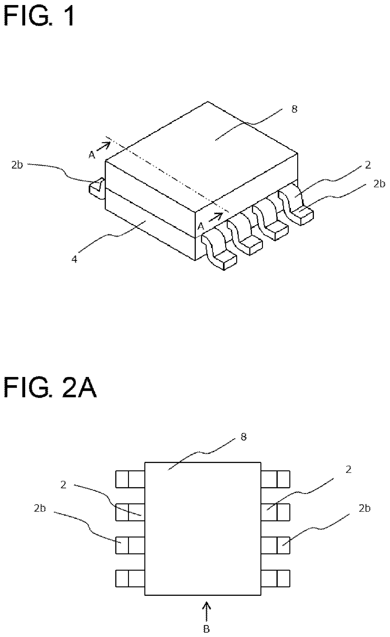
[0029]FIG. 1 is a bird's-eye view of a semiconductor device according to the present invention.
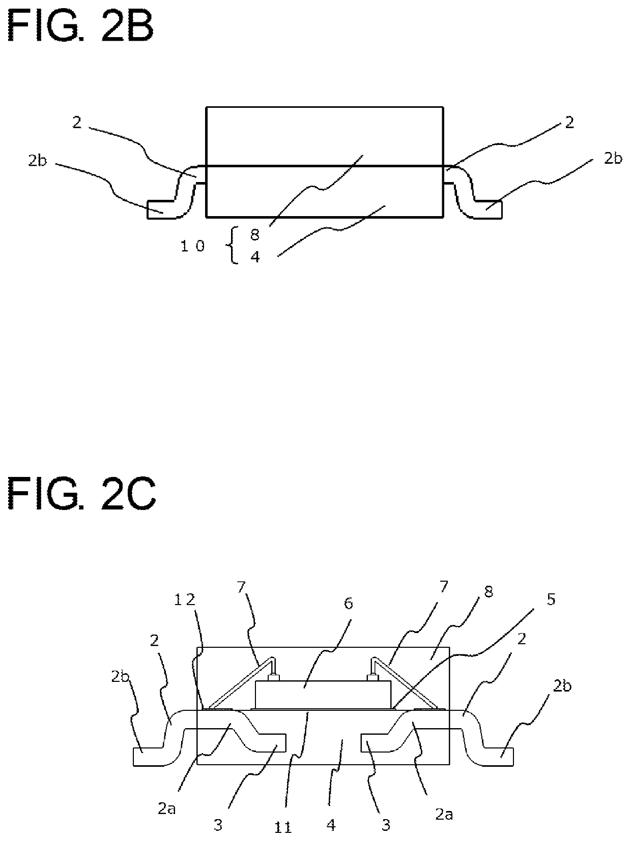
[0030]As illustrated in FIG. 1, the semiconductor device has a configuration in which a semiconductor element is covered with a first resin-encapsulating body 4 and a second resin-encapsulating body 8, and in which outer leads 2b which are part of leads 2 are exposed from the first resin-encapsulating body 4. Upper surfaces of the leads 2 are flush with an upper surface of the first resin-encapsulating body 4 and are brought into contact with a lower surface of the second resin-encapsulating body 8.
[0031]FIG. 2A to FIG. 2C are views from respective directions obtained from the bird's-eye view of FIG. 1. As illustrated in a top plan view of FIG. 2A, four outer leads 2b are provided to each of two opposing side surfaces of the semiconductor device. A view as seen in a direction indicated by the arrow B of a side surface adjacent to the two opposing side surfaces is FIG. 2B. The second resin-...
second embodiment
[0057]FIG. 10A to FIG. 15B are views for illustrating manufacturing steps of the semiconductor device according to the present invention.
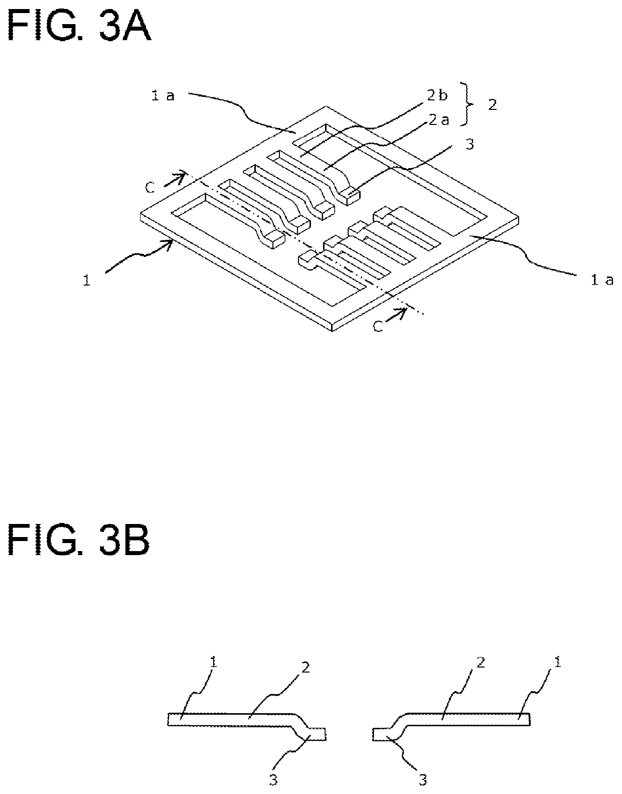
[0058]FIG. 10A and FIG. 10B are views for illustrating a lead frame used for the semiconductor device according to the second embodiment of the present invention. FIG. 10A is a bird's-eye view, and FIG. 10B is a cross-sectional view taken along the line G-G of FIG. 10A. A lead frame 1 includes a frame portion 1a which locates in the outer periphery of the lead frame 1, a plurality of leads 2 formed at inner sides of two frame members of the frame portion 1a, and the resin holding leads 9 formed at inner sides of the other two frame members adjacent to the above-mentioned two frame members. The leads 2 are connected respectively to two opposing frame members of the frame portion 1a, the resin holding leads 9 are connected respectively to the other two frame members adjacent to the two frame members, and the leads 2 and the resin holding leads 9 exte...
PUM
| Property | Measurement | Unit |
|---|---|---|
| shape | aaaaa | aaaaa |
| thickness | aaaaa | aaaaa |
| thermal stress | aaaaa | aaaaa |
Abstract
Description
Claims
Application Information
 - R&D
- Intellectual Property
- Life Sciences
- Materials
- Tech Scout
- Unparalleled Data Quality
- Higher Quality Content
- 60% Fewer Hallucinations
Browse by: Latest US Patents, China's latest patents, Technical Efficacy Thesaurus, Application Domain, Technology Topic, Popular Technical Reports.
© 2025 PatSnap. All rights reserved.Legal|Privacy policy|Modern Slavery Act Transparency Statement|Sitemap|About US| Contact US: help@patsnap.com