

SPUTTERING TARGET FOR OXIDE SEMICONDUCTOR, COMPRISING InGaO3(ZnO) CRYSTAL PHASE AND PROCESS FOR PRODUCING THE SPUTTERING TARGET
- Summary
- Abstract
- Description
- Claims
- Application Information
AI Technical Summary
Benefits of technology
Problems solved by technology
Method used
Image

Examples
examples
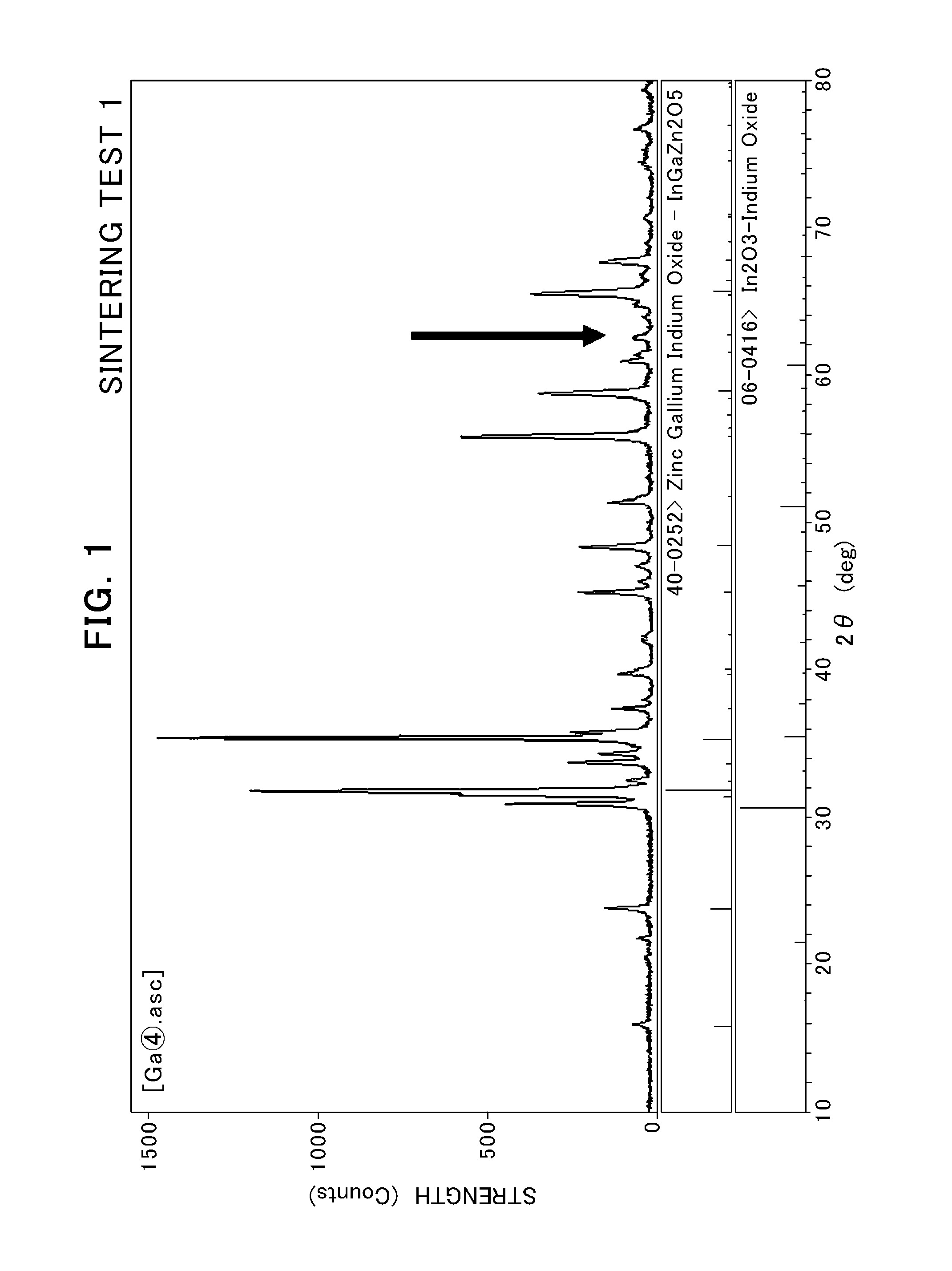
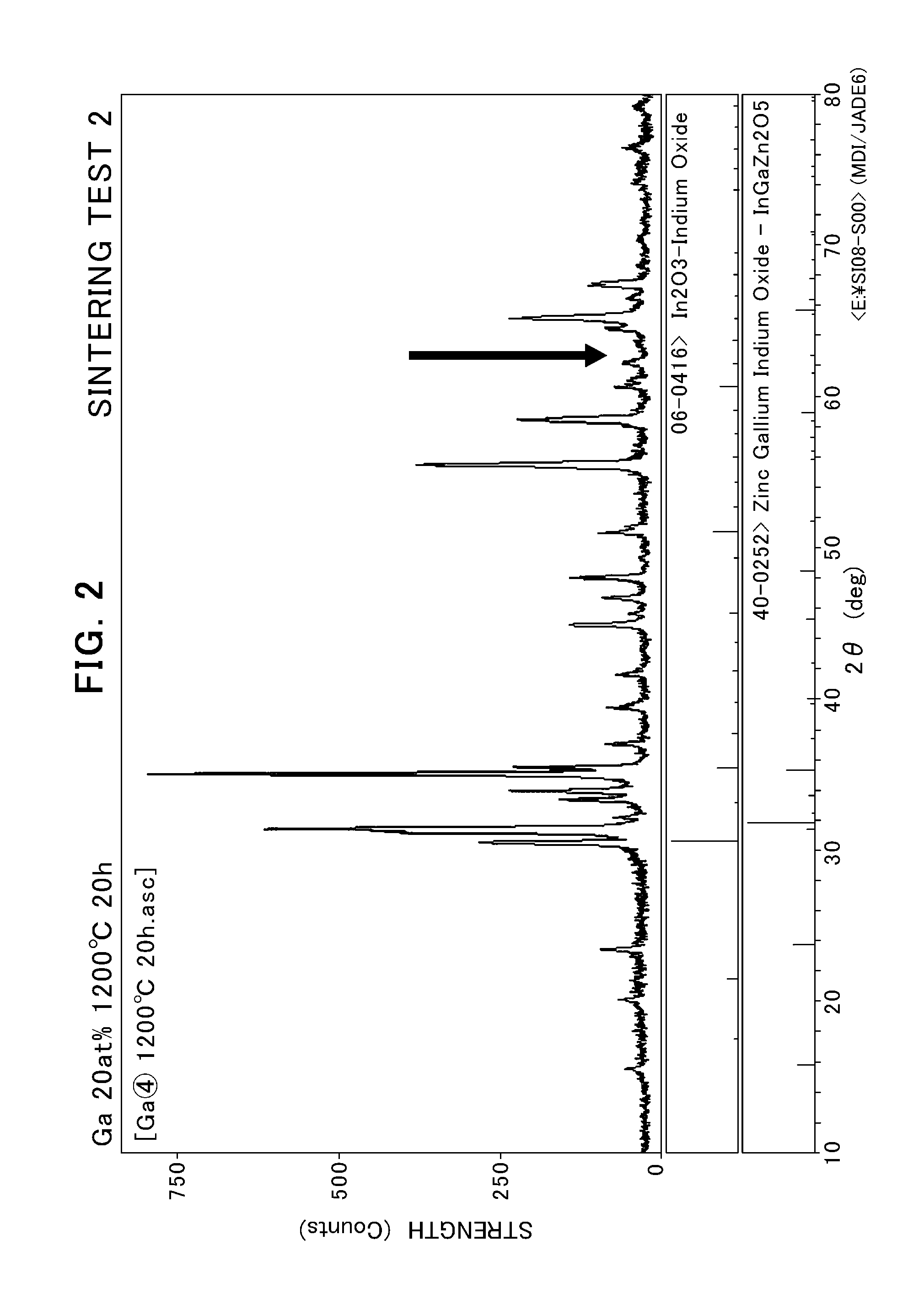
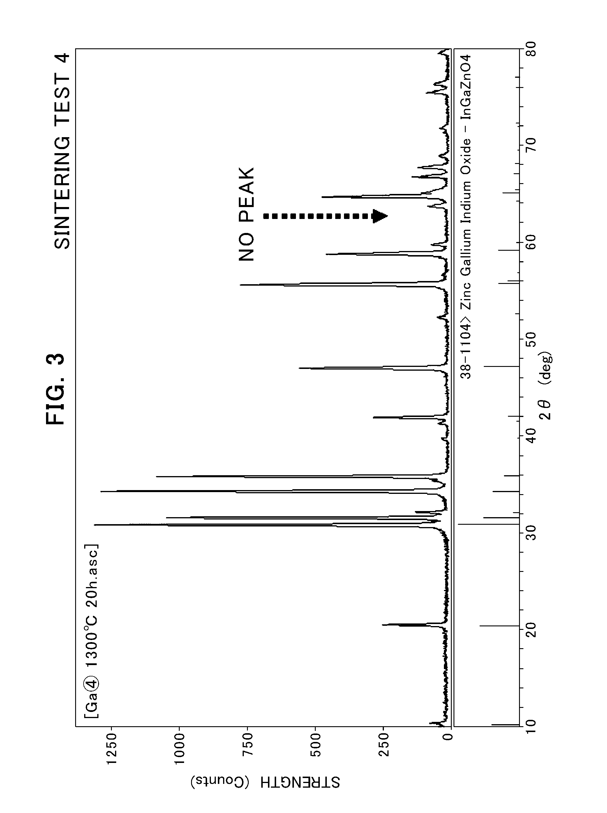
Sintering Tests 1-6
[0207]An In2O3 powder having specific surface area of 15 m2 / g, a Ga2O3 powder having specific surface area of 4 m2 / g, and a ZnO powder having specific surface area of 4 m2 / g were mixed, then an auxiliary agent was added, and then mixed and ground in a ball mil until each of crude powders has a particle size of 1 μm or less. Thus obtained slurry was picked out, and conducted to rapid-dry grinding using a spray dryer under slurry supply speed of 140 ml / min., hot air temperature of 140° C., and hot air amount of 8 Nm3 / min. The ground material was formed under pressure of 3 ton / cm2 using a cold isostatic press to obtain a formed body.
[0208]This formed body was placed in atmosphere and raising temperature at rate of 0.5° C. / min. up to 600° C., at rate of 1° C. / min. between 600 to 800° C., and at rate of 3° C. / min. between 800 to 1500° C. Then 1200° C. was kept for 2 hours to obtain a sintered body. Composition of thus obtained sintered body analyzed by ICP, and a cryst...
examples 2 to 16
, Comparative examples 1 to 9
[0253]Preparations and evaluations were the same as those of Example 1 except for composition and preparation conditions as shown in Tables.
example 17
Preparation of a Sputtering Target
[0254]As for crude powders, an indium oxide powder having an average median diameter (d50) of 1.5 μm, a gallium oxide powder having an average median diameter (d50) of 1.5 μm, and a zinc oxide powder having an average median diameter (d50) of 1.0 μm were weighed, and then mixed and ground by a wet-type medium agitating mill. The average median diameter (d50) after the grinding was set to 0.8 μm, and then dried by a spray dryer, filled in a metal mold, press formed by a cold press device to make a formed body, and then sintered under oxygen atmosphere at high temperature of 1300° C. for 20 hours. By using such steps, a sintered body for a sputtering target could be obtained without conducting a calcining step like as Example 1. The composition ratio of the obtained sintered body other than oxide analyzed by ICP was In:Ga:Zn=35:23:42.
[0255]A sintered body for a sputtering target was carved out from thus obtained sintered body. A side of the sintered b...
PUM
| Property | Measurement | Unit |
|---|---|---|
| Temperature | aaaaa | aaaaa |
| Temperature | aaaaa | aaaaa |
| Fraction | aaaaa | aaaaa |
Abstract
Description
Claims
Application Information