Organic light-emitting display device

a display device and organic light technology, applied in semiconductor devices, identification means, instruments, etc., can solve the problems of cracking or peeling of the vulnerable portion of the general oled display panel, and achieve the effect of preventing peeling, minimizing peeling, and minimizing peeling

Active Publication Date: 2022-08-16
LG DISPLAY CO LTD
View PDF2 Cites 0 Cited by
  • Summary
  • Abstract
  • Description
  • Claims
  • Application Information

AI Technical Summary

Benefits of technology

[0015]To address these limitations associated with the related art, the inventors have invented a novel structure of an OLED display panel, which is able to relieve stress in relation to compressive stress and tensile stress in an application environment in which the OLED display panel is flexed.
[0016]Various aspects of the present disclosure provide an improved organic light-emitting display device (also referred to as an OLED display device) having an improved structure that can minimize peeling of either an organic light-emitting layer or an encapsulation layer, which can be caused by repetitive bending stress in a flexing environment.
[0017]Also according to one or more embodiments of the present disclosure, there is provided an OLED display device in which peeling of either an organic light-emitting layer or an encapsulation layer, which may be caused by repetitive bending stress in a flexing environment, is minimized, so that the reliability of the OLED display device with respect to the flexing environment can be improved.
[0019]According to an aspect of the present disclosure, an OLED display panel having a structure able to minimize peeling of either an organic light-emitting layer or an encapsulation layer is provided. There, a pixel electrode is provided on a substrate, and a bank layer is provided on the pixel electrode to expose at least a portion of the pixel electrode, so that a pixel is defined by the exposed pixel electrode. The organic light-emitting and a common electrode are disposed on the exposed pixel electrode, and a first encapsulation layer and a second encapsulation layer are disposed on the common electrode. An anti-peeling pattern having a delta-shaped space is disposed on the bank layer. Accordingly, peeling of either the organic light-emitting layer or the encapsulation layer in the flexing environment can be minimized or prevented.
[0020]An OLED display device according to embodiments of the present disclosure can include an organic light-emitting element including a pixel electrode, an organic light-emitting layer, and a common electrode located on a substrate; and at least one encapsulation layer protecting the organic light-emitting element. The OLED display device can further include at least one anti-peeling pattern for the encapsulation layer, provided on a bank layer to expose the pixel electrode, with at least one side surface of the anti-peeling pattern having an inverted trapezoidal shape. As such, peeling of the encapsulation layer which may be caused by stress occurring in a flexing environment can be effectively minimized.
[0021]According to exemplary embodiments of the present disclosure, the anti-peeling pattern can minimize peeling of either the organic light-emitting layer or the encapsulation layer in a flexing environment in which the OLED display device is bent, so that the reliability of the OLED display device can be improved.

Problems solved by technology

A vulnerable portion of components of the general OLED display panel can be cracked or can be peeled from the substrate.

Method used


Image

  • Organic light-emitting display device
  • Organic light-emitting display device
  • Organic light-emitting display device

Examples


Embodiment Construction

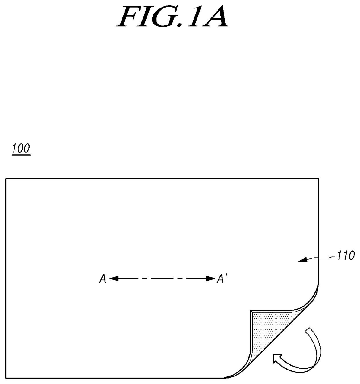
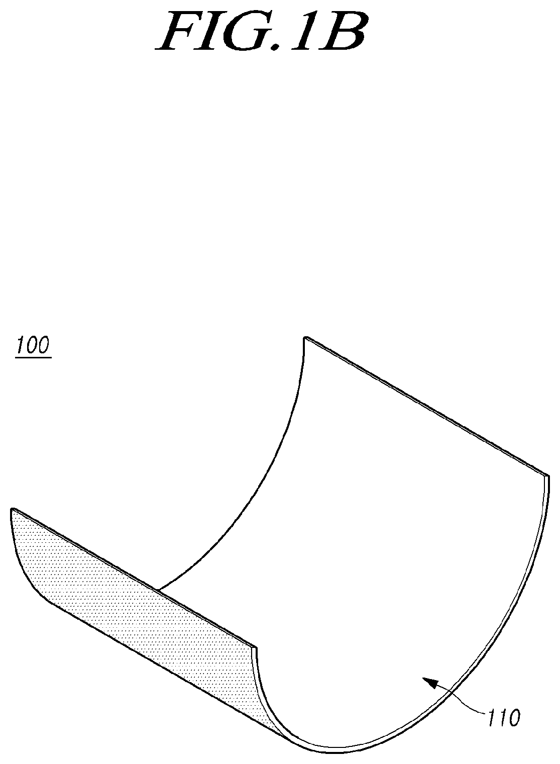
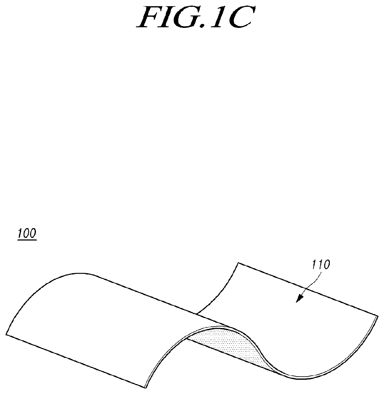
[0029]The advantages and features of the present disclosure and methods of the realization thereof will be apparent with reference to the accompanying drawings and detailed descriptions of the embodiments. The present disclosure should not be construed as being limited to the embodiments set forth herein and can be embodied in many different forms. Rather, these embodiments are provided so that the present disclosure will be thorough and complete, and will fully convey the scope of the present disclosure to those having ordinary knowledge in the technical field. The scope of the present disclosure shall be defined by the appended Claims.

[0030]The shapes, sizes, ratios, angles, numbers, and the like, inscribed in the drawings to illustrate exemplary embodiments are illustrative only, and the present disclosure is not limited to the embodiments illustrated in the drawings. Throughout this document, the same reference numerals and symbols will be used to designate the same or like comp...


PUM

PropertyMeasurementUnit
distanceaaaaaaaaaa
widthaaaaaaaaaa
widthaaaaaaaaaa

Abstract

An organic light-emitting display device includes an anti-peeling pattern. An organic light-emitting element including a pixel electrode, an organic light-emitting layer, and a common electrode is disposed on a substrate. A bank layer is disposed on the pixel electrode so as to expose at least a portion of the pixel electrode. The anti-peeling pattern having at least one delta-shaped space is disposed on the bank layer. The anti-peeling pattern, disposed on the bank layer, minimizes peeling of the encapsulation layer that can be caused by either compressive or tensile stress generated by bending in a flexing environment in which the organic light-emitting display device is used.

Description

CROSS REFERENCE TO RELATED APPLICATION[0001]This application claims priority to Korean Patent Application No. 10-2018-0134110, fled on Nov. 5, 2018, which is hereby incorporated by reference for all purposes as if fully set forth herein.BACKGROUNDField[0002]Embodiments of the present disclosure relate to an organic light-emitting display device and, more particularly, to an organic light-emitting display device having a structure able to minimize peeling of either an organic light-emitting layer or an encapsulation layer provided on a pixel electrode in a flexing environment, in which the organic light-emitting display device is folded and bent.Description of Related Art[0003]Organic light emitting display devices, also referred to as organic light-emitting diode (OLED) display devices, can be fabricated to have a thin and light profile, since OLEDs, i.e., self-light-emitting devices, are used therein, and thus, a separate light source is not required, unlike liquid crystal display ...

Claims


Application Information

Patent Timeline
Patent Type & Authority Patents(United States)
IPC IPC(8): H01L27/32H01L51/52H01L51/00
CPCH01L51/5253H01L27/3246H01L51/0097G09F9/301H10K59/12H10K50/84H10K59/122H10K50/844H10K2102/311H10K59/00H10K50/805H10K77/111
Inventor LEE, KYOUNGMOOKCHOI, NACKBONGKIM, DONGYULHAN, MYUNGWOOBAE, YEONGYEONG
Owner LG DISPLAY CO LTD
Why Eureka
Try Eureka