
Semiconductor package and method of manufacturing the same
a technology of semiconductor and semiconductor package, which is applied in the direction of semiconductor devices, semiconductor/solid-state device details, electrical apparatus, etc., can solve the problems of difficult and/or expensive manufacturing of such voltage regulators, and achieve the effect of reducing the size of the package, minimizing or improving the operating characteristics of the ivr chip
- Summary
- Abstract
- Description
- Claims
- Application Information
AI Technical Summary
Benefits of technology
Problems solved by technology
Method used
Image

Examples
Embodiment Construction
[0018]Exemplary embodiments of the inventive concept will be described more fully hereinafter with reference to the accompanying drawings. Like reference numerals may refer to like elements throughout the accompanying drawings, and redundant descriptions thereof may be omitted.
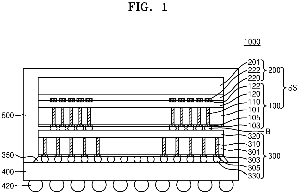
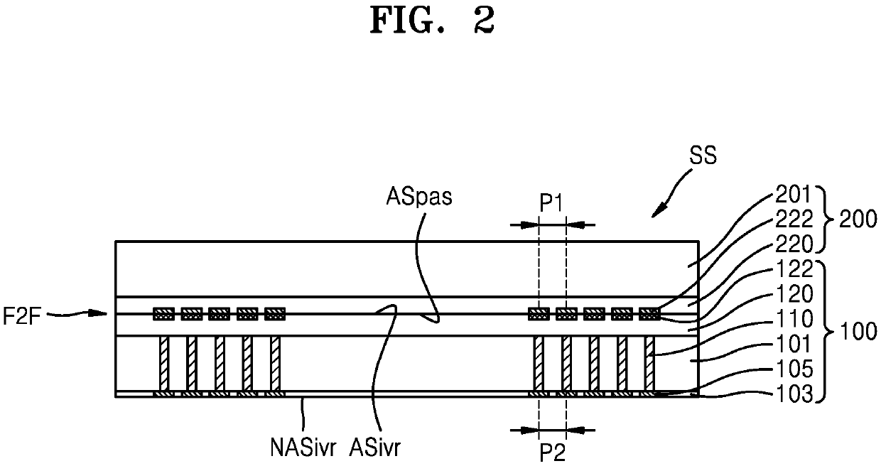
[0019]FIG. 1 is a cross-sectional view of a semiconductor package 1000 according to an exemplary embodiment. FIG. 2 is a cross-sectional view showing a stack structure SS including an integrated voltage regulator (IVR) chip 100 and a passive element chip 200 in the semiconductor package 1000 of FIG. 1. The term ‘chip’ may refer to a semiconductor chip.
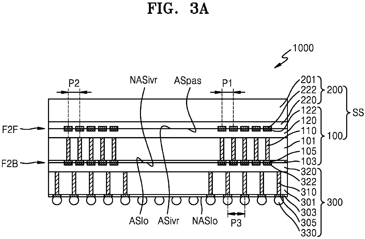
[0020]Referring to FIGS. 1 and 2, the semiconductor package 1000 according to an exemplary embodiment may include a logic chip 300, the stack structure SS, a package substrate 400, and a sealing material 500.
[0021]As shown in FIG. 1, in an exemplary embodiment, the stack structure SS may be stacked on the package substrate 400 in a configuration in which the stac...
PUM
| Property | Measurement | Unit |
|---|---|---|
| voltage | aaaaa | aaaaa |
| voltages | aaaaa | aaaaa |
| input current | aaaaa | aaaaa |
Abstract
Description
Claims
Application Information