

Exfoliating method, transferring method of thin film device, and thin film device, thin film integrated circuit device, and liquid crystal display device produced by the same
a transfer method and technology of thin film, applied in the direction of instruments, semiconductor devices, optics, etc., can solve the problems of deterioration or damage, large transparent substrates cannot be produced from materials with large thickness, and large thickness, etc., to achieve easy exfoliation (ablation), short time, and no deterioration or damage
Inactive Publication Date: 2002-10-10
SAMSUNG ELECTRONICS CO LTD
View PDF0 Cites 227 Cited by
- Summary
- Abstract
- Description
- Claims
- Application Information
AI Technical Summary
Benefits of technology
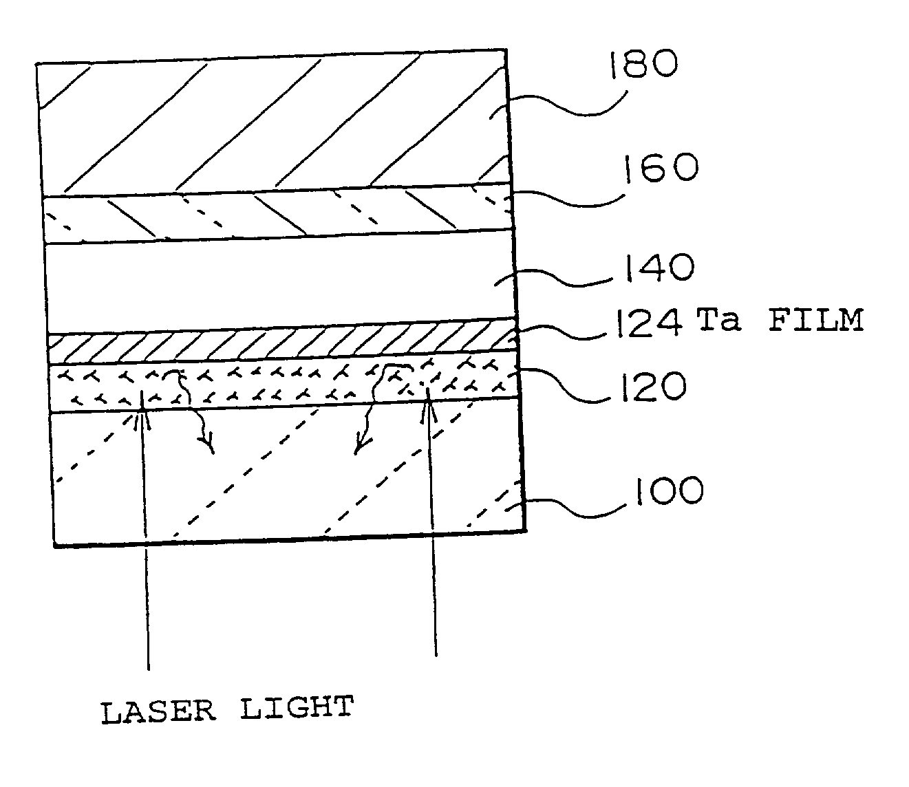
[0030] In accordance with the present invention, for example, a separation layer having optical absorption characteristics is provided on a substrate having high reliability in device production, and thin film devices such as TFTs and the like are formed on the substrate. Next, although not for limitation, the thin film devices are adhered to a given transfer member, for example, with an adhesive layer, so as to cause an exfoliation phenomenon in the separation layer, which results in a decrease in adhering between the separation layer and the substrate. The substrate is detached from the thin film devices by the force applied to the substrate. A given device with high reliability can be thereby transferred or formed onto any transfer members.
[0236] When the substrate 1 is composed of an expensive or rare material such as quartz glass, it is preferable that the substrate 1 be reused (recycled). In other words, the present invention is applicable to a substrate to be reused, and thus is highly useful.
Problems solved by technology
For example, in the production process with high temperature treatment, quartz glass or heat-resisting glass is used, however, they are rare and very expensive materials, and a large transparent substrate can barely be produced from the material.
Further, quartz glass and heat-resisting glass are fragile, easily broken, and heavy.
These are severe disadvantages when a substrate provided with thin film devices such as TFTs is mounted into electronic units.
There is a gap between restriction due to process conditions and preferred characteristics required for products, hence it is significantly difficult to satisfy both the restriction and characteristics.
Method used
View moreImage
Smart ImageViewing Examples

Examples
example 13
[0181] A thin film transistor was transferred as in Example 2, but a transparent AS resin substrate (glass transition point: 70 to 90.degree. C.) as the transfer member was used.
example 14
[0182] A thin film transistor was transferred as in Example 3, but a transparent polymethyl methacrylate substrate (glass transition point: 70 to 90.degree. C.) as the transfer member was used.
example 15
[0183] A thin film transistor was transferred as in Example 5, but a transparent polyethylene terephthalate substrate (glass transition point: 67.degree. C.) as the transfer member was used.
Login to View More PUM
| Property | Measurement | Unit |
|---|---|---|
| softening point | aaaaa | aaaaa |
| wavelength | aaaaa | aaaaa |
| wavelength | aaaaa | aaaaa |
Abstract
A method for transferring a thin film device on a substrate onto a transfer member, includes a step for forming a separation layer on the substrate, a step for forming a transferred layer including the thin film device on the separation layer, a step for adhering the transferred layer including the thin film device to the transfer member with an adhesive layer therebetween, a step for irradiating the separation layer,with light so as to form internal and / or interfacial exfoliation of the separation layer, and a step for detaching the substrate from the separation layer.
Description
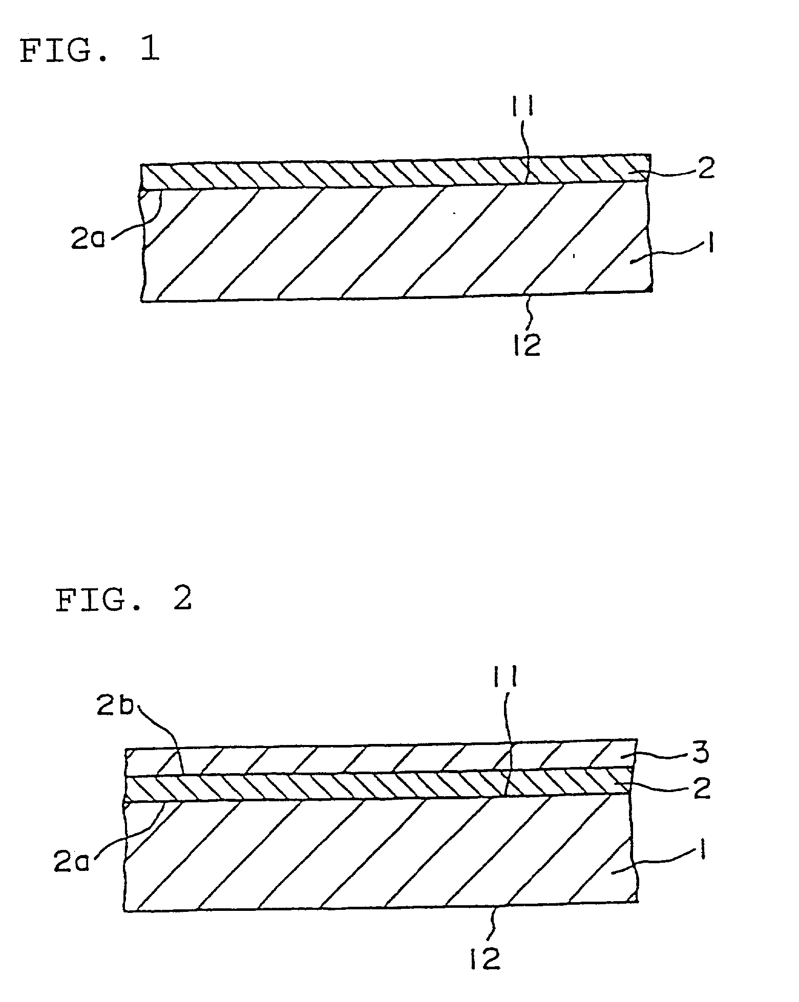
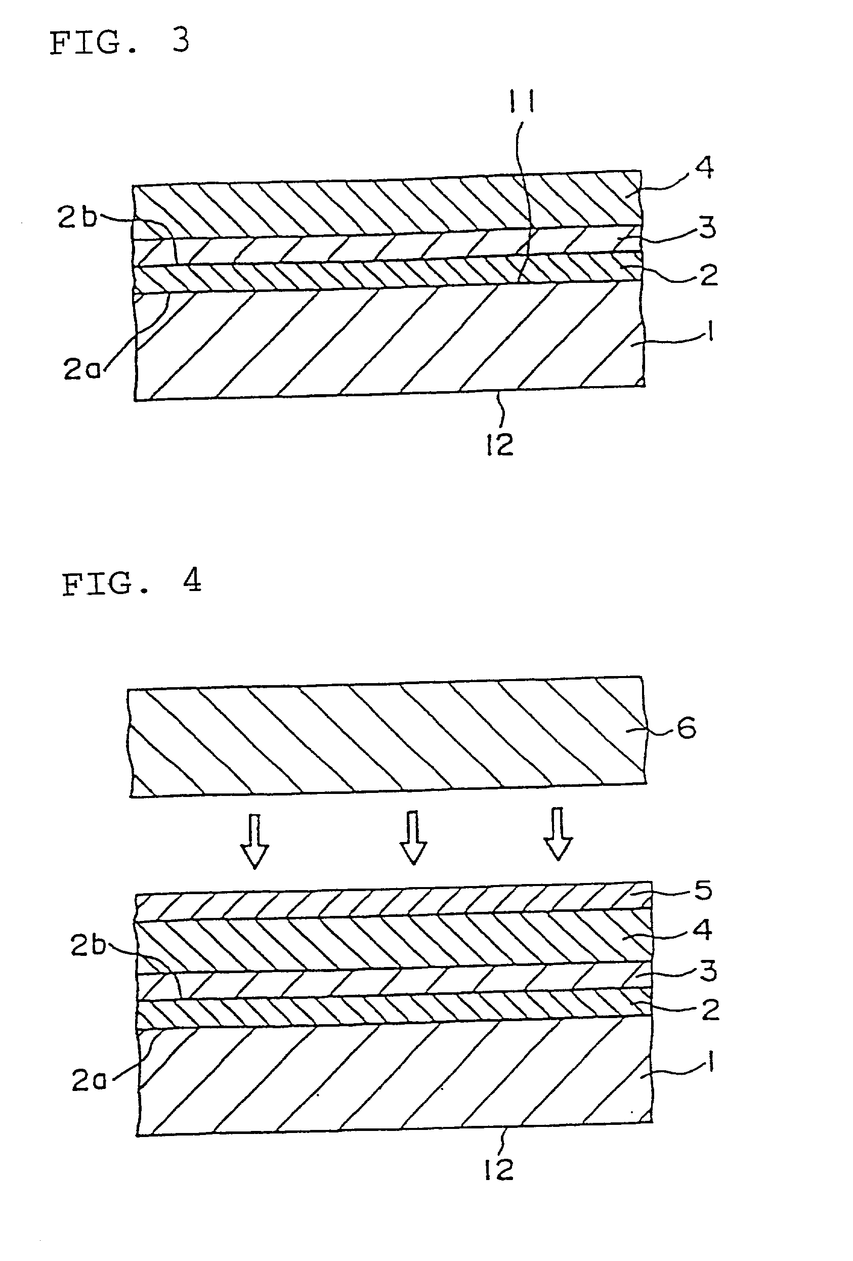
[0001] The present invention relates to a method for exfoliating a detached member, and in particular, a transferring method for exfoliating a transferred layer comprising a thin film such as a functional thin film and for transferring it onto a transfer member such as a transparent substrate. Also, the present invention relates to a transferring method of a thin film device, a thin film device, a thin film integrated circuit device, and a liquid crystal display device produced using the same.[0002] Production of liquid crystal displays using thin film transistors (TFTs), for example, includes a step for forming thin film transistors on a transparent substrate by a CVD process or the like.[0003] The thin film transistors are classified into those using amorphous silicon (a--Si) and those using polycrystalline silicon (p--Si), and those using polycrystalline silicon are classified into those formed by a high temperature process and those formed by a low temperature process.[0004] Sin...
Claims
Login to View More Application Information
Patent Timeline
 Patent Type & AuthorityApplications(United States)
IPC IPC(8): G02F1/1362G02F1/1368H01L21/68H01L21/762H01L21/77H01L21/84H01L27/12
CPCG02F1/13454G02F1/1368G02F2001/13613H01L21/6835H01L21/76251H01L2221/68363H01L21/76259H01L27/1214H01L27/1266H01L29/78603H01L2221/68359H01L21/76254G02F1/13613
InventorSHIMODA, TATSUYAINOUE, SATOSHIMIYAZAWA, WAKAO
OwnerSAMSUNG ELECTRONICS CO LTD