Liquid crystal display device and manufacturing method of the same

a technology of liquid crystal display and manufacturing method, which is applied in semiconductor devices, instruments, optics, etc., can solve the problems of increased resistance, deterioration of display qualities, signal delay, etc., and achieve the effect of suppressing the occurrence of disconnection failures of the second wiring in the upper layer side, reducing the risk of disconnection failure, and improving the adhesion of the first wiring to the insulating substra

Inactive Publication Date: 2006-09-21
VISTA PEAK VENTURES LLC
View PDF4 Cites 28 Cited by
  • Summary
  • Abstract
  • Description
  • Claims
  • Application Information

AI Technical Summary

Benefits of technology

[0012] According to the present invention, in the TFT substrate, the first wiring (or the first wiring and the light-shielding film) made from the Cu layer in the lower layer side is formed in the groove on a surface of the insulating substrate. The TFT substrate is made into a structure where the barrier metal film is covering the surroundings of the Cu layer. The mutual reactions between the Cu layer and Si in the insulating substrate made of a glass substrate or the like can be suppressed and resistances to chemicals and corrosion of the first wiring can be improved. Furthermore, adhesion of the first wiring to the insulating substrate can also be improved. Additionally, since the first wiring is embedded in the groove, occurrence of the disclination defects and disconnection failures of the second wiring in the upper layer side can be suppressed by reducing the side difference in level due to the presence of the first wiring Moreover, in the LCD device of the present invention, it is possible to lower the resistance of a lower layer wiring by using a groove wiring made of Cu metal for the lower layer wiring of the TFT substrate and to suppress signal delays in the lower layer wiring. In the present invention, by using the TFT substrate having such a lower layer wiring structure, it is possible to manufacture a LCD device with large size, high density, large aperture ratio and improved display qualities.

Problems solved by technology

As a result, signal delays occur and display qualities becomes prone to deterioration.
However, when wirings become narrow, the resistance increases similarly to the case described before and the display qualities deteriorate due to the signal delays.
Since aluminum (Al), which has hitherto been used as a material for the gate wirings, has an especially high resistance, it is impossible to obtain an LCD device with a high image quality due to a signal delay at the gate wiring.
However, due to mutual reactions between Cu and oxide silicon (SiO2), silicon nitride (SiN), or the like in Si-containing films, film qualities tend to deteriorate when Cu is used as the material for wirings.
Moreover, because of poor resistances to chemicals and corrosion, Cu is likely to be etched during manufacturing steps of the TFT substrate.
Furthermore, there is a problem where Cu cannot be used as a single layer due to a drawback of Cu such as its poor adhesion to substrates.
As a result, there was a problem that disclination defects due to disorder of liquid crystal orientation and disconnection failures of an upper layer wiring tend to occur readily.

Method used


Image

  • Liquid crystal display device and manufacturing method of the same
  • Liquid crystal display device and manufacturing method of the same
  • Liquid crystal display device and manufacturing method of the same

Examples


Embodiment Construction

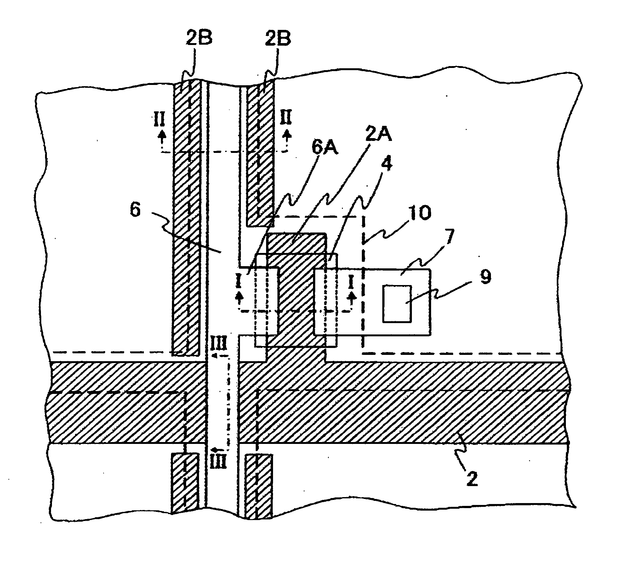
[0025] Embodiments of the LCD device of the present invention will be described with reference to drawings. A structure of a TFT substrate as an example of a first substrate for display of the LCD device of the present invention is shown in FIG. 3 and FIGS. 4A to 4C. A gate wiring 2 is formed in a groove on the surface of the insulating substrate 1 made of a glass substrate or a plastic substrate. Incidentally, polycarbonates, polyether sulfones, polyarylates, or the like can be used for the plastic substrate. A drain wiring 6 is formed on the insulating substrate 1 in a manner to be perpendicular to the gate wiring 2. A TFT as a switching element is arranged in a vicinity of a crossing portion between the gate wiring 2 and the drain wiring 6. The TFT is provided with a gate electrode 2A formed in a groove 12 at the surface of the insulating substrate 1 and a gate insulating film 3 formed on the insulating substrate 1 including the gate electrode 2A as shown in FIG. 4A. The gate ins...


PUM

PropertyMeasurementUnit
thicknessaaaaaaaaaa
thicknessaaaaaaaaaa
depthaaaaaaaaaa

Abstract

An active matrix substrate or TFT substrate is provided with a lower layer wiring with a groove wiring structure covering surroundings of a copper layer with a barrier metal film is formed by forming a groove at an insulating substrate and depositing the barrier metal film and the copper layer in this groove. This groove wiring structure is used for a TFT substrate of a liquid crystal display (LCD) device. It is possible to manufacture an LCD device with large size, high density, a large aperture ratio and in which the disclination defects originating from a different in level of the lower layer wiring and an occurrence of disconnection failures in an upper layer wiring are suppressed.

Description

BACKGROUND OF THE INVENTION [0001] 1. Field of the Invention [0002] The present invention relates to a liquid crystal display (LCD) device and its manufacturing method. In particular, the present invention relates to a structure of a substrate for display device of the LCD device and its manufacturing method. [0003] 2. Description of the Prior Art [0004] In recent years, an active-matrix type LCD device is widely used as a display with high resolution. Such LCD device has a liquid crystal sandwiched between an active matrix substrate as a first substrate and an opposite substrate as a second substrate. A typical example of the active matrix substrate is provided with switching elements such as thin film transistors (TFTs) at each of plurality of pixels and the opposite substrate is provided with color filters and a black matrix. In this LCD device, orientation directions of liquid crystal molecules are changed by an electric field between electrodes provided on the active matrix sub...

Claims


Application Information

Patent Timeline
Patent Type & Authority Applications(United States)
IPC IPC(8): G02F1/136
CPCG02F1/133305G02F1/136209G02F1/136286H01L27/124G02F2001/136295H01L27/1218G02F2001/13629G02F1/13629G02F1/136295G02F1/136
Inventor YASUDA, KYOUNEISUZUKI, SEIJI
Owner VISTA PEAK VENTURES LLC
Why Eureka
Try Eureka