Conductivity variable composition, conductivity variable laminated body, and conductive pattern formed body

a technology of conductivity variable and composition, which is applied in the direction of photosensitive materials, natural mineral layered products, instruments, etc., can solve the problems of complex production methods, high equipment cost, running cost or the like, and achieve the effect of improving the conductivity, improving the conductivity, and improving the entire surface of the organic el elemen

Inactive Publication Date: 2006-10-05
DAI NIPPON PRINTING CO LTD
View PDF17 Cites 5 Cited by
  • Summary
  • Abstract
  • Description
  • Claims
  • Application Information

AI Technical Summary

Benefits of technology

[0008] According to the present invention, since the above-mentioned insulating particle has an organic material adhered on the circumference of a conductive inorganic material, particles having the insulation property can be provided so that a conductivity variable composition can be provided without the conductivity. Moreover, since a photocatalyst is contained in the above-mentioned conductivity variable composition, the above-mentioned organic material can be eliminated from the circumference of the above-mentioned conductive inorganic material by an action of the photocatalyst by directing the energy to the conductivity variable composition so that the conductivity variable composition can be provided with the conductivity. Therefore, according to the present invention, a conductivity variable composition capable of easily changing the conductivity by the energy irradiation can be provided.
[0010] According to the present invention, since the above-mentioned conductivity variable layer contains the above-mentioned insulating particle, a layer having the insulation property can be provided. Moreover, since the above-mentioned organic material can be eliminated from the circumference of the conductive inorganic material of the above-mentioned insulating particle by applying an action of the photocatalyst accompanied by the energy irradiation to the conductivity variable layer, the conductivity can be realized in the conductivity variable layer. Therefore, by applying an action of the photocatalyst in a pattern to the above-mentioned conductivity variable layer, a conductive pattern and an insulating pattern can be easily formed. Thereby, for example a wiring of a wiring substrate or the like can be formed highly precisely.
[0011] In the above-mentioned invention, the above-mentioned conductivity variable layer may contain a photocatalyst. Thereby, the conductivity of the conductivity variable layer can be easily changed by an action of the photocatalyst in the conductivity variable layer by directing the energy to the above-mentioned conductivity variable layer.
[0015] According to the present invention, since the organic EL layer is formed on the above-mentioned conductive pattern formed body having a conductive pattern, the electric characteristic of the organic EL element can be provided preferably. Here, in general, in the case the conductivity of the organic EL element entire surface is improved, at the time of carrying out the moving video image display, the other pixels other than the designated pixels may also emit a light beam. However, according to the present invention, the conductive pattern can be formed so as to improve the conductivity for each of the above-mentioned pixels so that an organic EL element capable of emitting a light beam in a highly precise pattern can be provided. Moreover, since the photocatalyst is contained in the above-mentioned conductivity variable layer, a conductivity variable layer having the function of transporting the electron or the hole can be provided. Therefore, it is advantageous in that the above-mentioned conductivity variable layer can be used as a hole transporting layer or an electron transporting layer.
[0016] According to the present invention, it is advantageous in that a conductivity variable composition capable of easily realizing the conductivity by directing the energy can be provided.

Problems solved by technology

Therefore, a problem is involved in that the production method is complicated.
Moreover, since the above-mentioned metal layer is formed by in general a CVD, sputtering or the like so as to require vacuum based equipment and equipment capable of carrying out the high temperature treatment, and thus a problem is involved in that the burden of the equipment cost, the running cost or the like is extremely heavy.
Furthermore, another problem is also involved in terms of the environment in that the waste liquid generated in a large quantity at the time of the development is hazardous so as to require the process before discharging the same to the outside or the like.
Moreover, according to the above-mentioned mask deposition method, since the electrode material or the like needs to be deposited, a problem is involved in that vacuum based equipment or the like is needed so that the burden of the equipment cost, the running cost or the like is heavy while also, the productivity is low.

Method used


Image

  • Conductivity variable composition, conductivity variable laminated body, and conductive pattern formed body
  • Conductivity variable composition, conductivity variable laminated body, and conductive pattern formed body
  • Conductivity variable composition, conductivity variable laminated body, and conductive pattern formed body

Examples


first embodiment

(1) First Embodiment

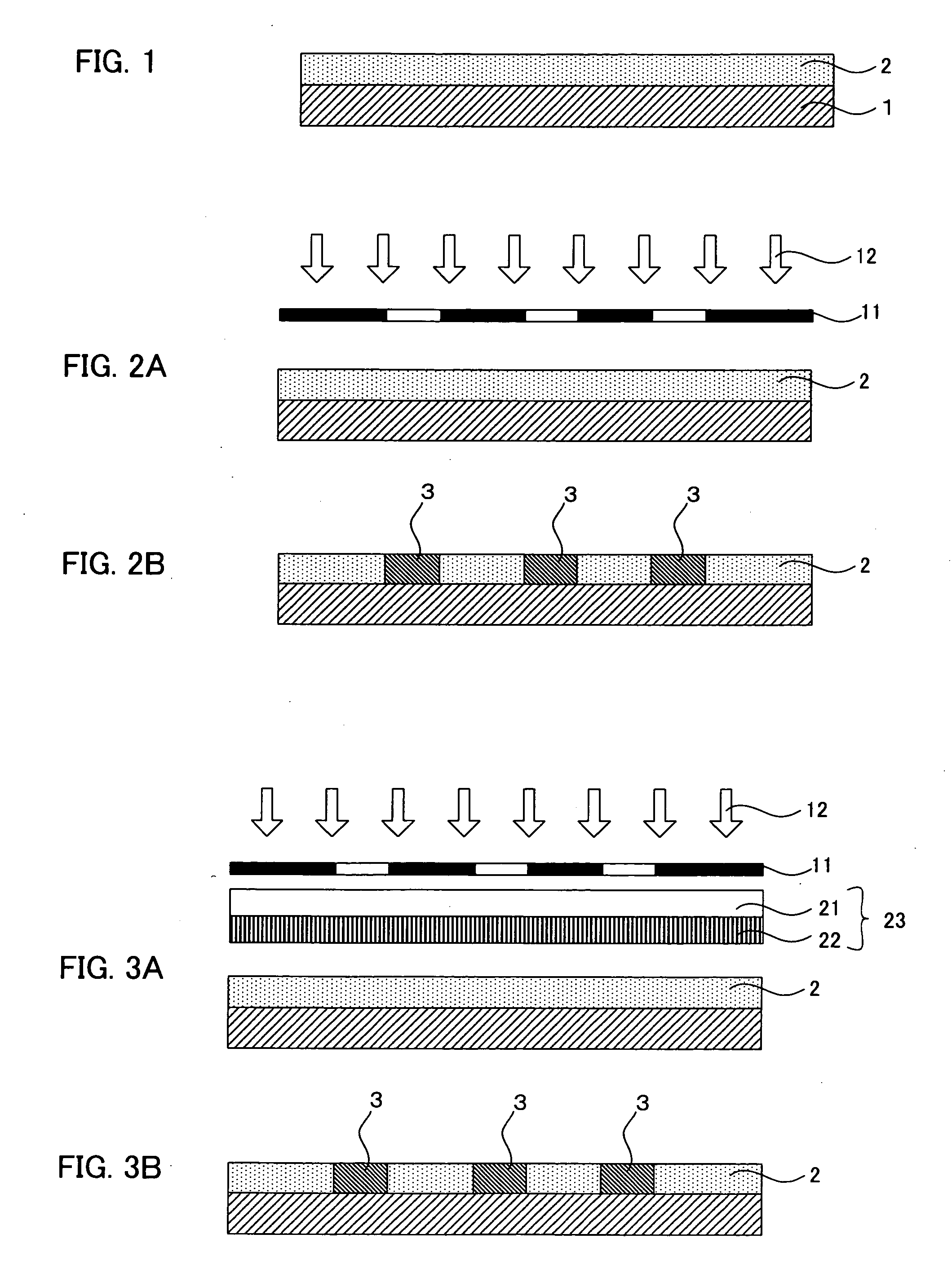
[0094] First, the method for forming the conductive pattern and the insulating pattern in the case the photocatalyst is contained in the above-mentioned conductivity variable laminated body will be explained. In the case the photocatalyst is contained in the conductivity variable laminated body, that is, the photocatalyst is contained in the above-mentioned conductivity variable layer, or the photocatalyst containing layer is formed between the conductivity variable layer and the base material, or the like, the conductive pattern and the insulating pattern can be formed by directing an energy in a pattern to the conductivity variable layer of the conductivity variable laminated body.

[0095] At the time, the energy to be directed is a concept including irradiation of any energy line as long as it can eliminate the organic material adhered on the circumference of the above-mentioned conductive inorganic material by exciting the above-mentioned photocatalyst so that...

second embodiment

(2) Second Embodiment

[0100] Next, the method for forming the conductive pattern and the insulating pattern in the case the photocatalyst is not contained in the above-mentioned conductivity variable laminated body will be explained. In the case the photocatalyst is not contained in the conductivity variable laminated body, as mentioned above, by directing the energy with the photocatalyst containing layer containing the photocatalyst and the above-mentioned conductivity variable layer disposed facing with each other, the conductive pattern and insulating pattern can be formed.

[0101] As to the photocatalyst containing layer side substrate having the photocatalyst containing layer used for the formation of the conductive pattern and the insulating pattern, in general, it may be one including a base body and a photocatalyst containing layer formed on the base body. A light shielding part may be formed on the photocatalyst containing layer or base body. In this case, by directing the e...

example

[0170] Hereinafter, the present invention will be explained further specifically with reference to the examples.

[0171] At a room temperature, 5 parts by weight of a pyrocarbonate dibutyl produced by Tokyo Chemical Industry Co., Ltd. dissolved in a minute amount of a tetrahydro furan produced by KANTO KAGAKU. and 95 parts by weight of a solid component of a silver colloid produced by NIPPON PAINT Co., Ltd. were agitated for 12 hours. Thereafter, by eliminating a minute amount of unnecessary precipitates and aggregates by the filtration under reduced pressure, a silver dispersion treated with the dibutoxy carbonyl was obtained.

[0172] By gradually adding a titanium oxide coating solution (TKS-201) produced by ISHIHARASANGYOKAISHA, LTD. to the silver dispersion while agitating the dispersion so as to have a 2:8 weight ratio by the solid component ratio, and furthermore, eliminating a minute amount of unnecessary precipitates and aggregates by the filtration under reduced pressure, a d...


PUM

PropertyMeasurementUnit
particle sizeaaaaaaaaaa
excitation wavelengthaaaaaaaaaa

Abstract

The main object of the present invention is to provide a conductive pattern formed body with a conductive pattern formed efficiently and highly precisely in a simple process, a conductivity variable laminated body used for formation of the conductive pattern, and the like. To attain the object, the invention provides a conductivity variable composition characterized by containing insulating particle including a conductive inorganic material and an organic material adhered on the circumference of the conductive inorganic material, and a photocatalyst.

Description

BACKGROUND OF THE INVENTION [0001] 1. Field of the Invention [0002] The present invention relates to a conductive pattern formed body having a highly precise conductive pattern, to be used for formation of for example an organic electroluminescent (hereinafter it is also referred to as “EL”) element and a wiring substrate, a conductivity variable laminated body which is capable of easily forming the conductive pattern formed body or the like. [0003] 2. Description of the Related Art [0004] Conventionally, a photolithography method, a mask deposition method or the like has been generally used for formation of a conductive pattern of a conductive pattern formed body used for a wiring substrate or the like. However, according to the above-mentioned photolithography method, various processes such as; a process of forming a metal layer on a substrate, a process of forming a photoresist layer on a metal layer, a process of exposing the photoresist layer, a process of developing the photor...

Claims


Application Information

Patent Timeline
Patent Type & Authority Applications(United States)
IPC IPC(8): B32B27/08
CPCG03F7/0047H01L27/3239H01L51/0015H01L51/0021H01L51/5048Y10T428/2991H05K1/092H05K3/105H05K2201/0224H05K2203/1142H01L51/5088Y10T428/31928H10K59/221H10K71/211H10K71/60H10K50/14H10K50/17G03C1/72H01L21/288H01L21/3205H01L21/768H05B33/10H10K59/00H10K50/00H10K71/00
Inventor KOBAYASHI, YOSHIHIROITOH, KIYOSHI
Owner DAI NIPPON PRINTING CO LTD
Why Eureka
Try Eureka