Analog vertical sub-sampling in an active pixel sensor (APS) image sensor

an image sensor and active pixel technology, applied in the field of analog vertical subsampling in an active pixel sensor (aps) image sensor, can solve the problems of image with artifacts, no or minimal power saving, and averaging in the digital domain

Active Publication Date: 2007-10-04
APTINA IMAGING CORP +1
View PDF2 Cites 194 Cited by
  • Summary
  • Abstract
  • Description
  • Claims
  • Application Information

AI Technical Summary

Benefits of technology

[0004] In one embodiment, an integrated circuit includes an active pixel sensor (APS) image sensor comprising an array of pixel circuits corresponding to rows and columns of pixels, a plurality of amplifiers that buffer signals output by the array of pixel circuits, and a plurality of sample and hold circuits that read the buffered signals. The integrated circuit further includes a routing mechanism positioned between the array of pixel circuits and the plurality of amplifiers, and a controller that selects sets of the pixels circuits for sampling. The controller is configured to control the routing mechanism to couple each pixel circuit in a set to a different one of the amplifiers during a normal mode of operation, and to couple each pixel circuit of a subset of pixel circuits in a first set of pixel circuits to a different amplifier of a first subset of the amplifiers, to couple each pixel circuit of a subset of pixel circuits in a second set of pixel circuits to a different amplifier of a second subset of the amplifiers, and to couple the amplifiers of the first and second subsets of amplifiers in pairs to a common one of the sample and hold circuits during a sub-sampling mode of operation.

Problems solved by technology

Unfortunately, a drawback of conventional sub-sampling methods is that video information on skipped pixels is discarded resulting in an image with artifacts, particularly in scenes with considerable contrast.
This results in a pleasing image, but provides no or minimal savings in power.
Averaging in the digital domain can add noise to the final image.
Also, prior systems underutilize chip resources and consume needless power.

Method used


Image

  • Analog vertical sub-sampling in an active pixel sensor (APS) image sensor
  • Analog vertical sub-sampling in an active pixel sensor (APS) image sensor
  • Analog vertical sub-sampling in an active pixel sensor (APS) image sensor

Examples


Embodiment Construction

[0010] In the following detailed description of the preferred embodiments, reference is made to the accompanying drawings, which form a part hereof, and in which is shown by way of illustration specific embodiments in which the invention may be practiced. It is to be understood that other embodiments may be utilized and structural or logical changes may be made without departing from the scope of the present invention. The following detailed description, therefore, is not to be taken in a limiting sense, and the scope of the present invention is defined by the appended claims.

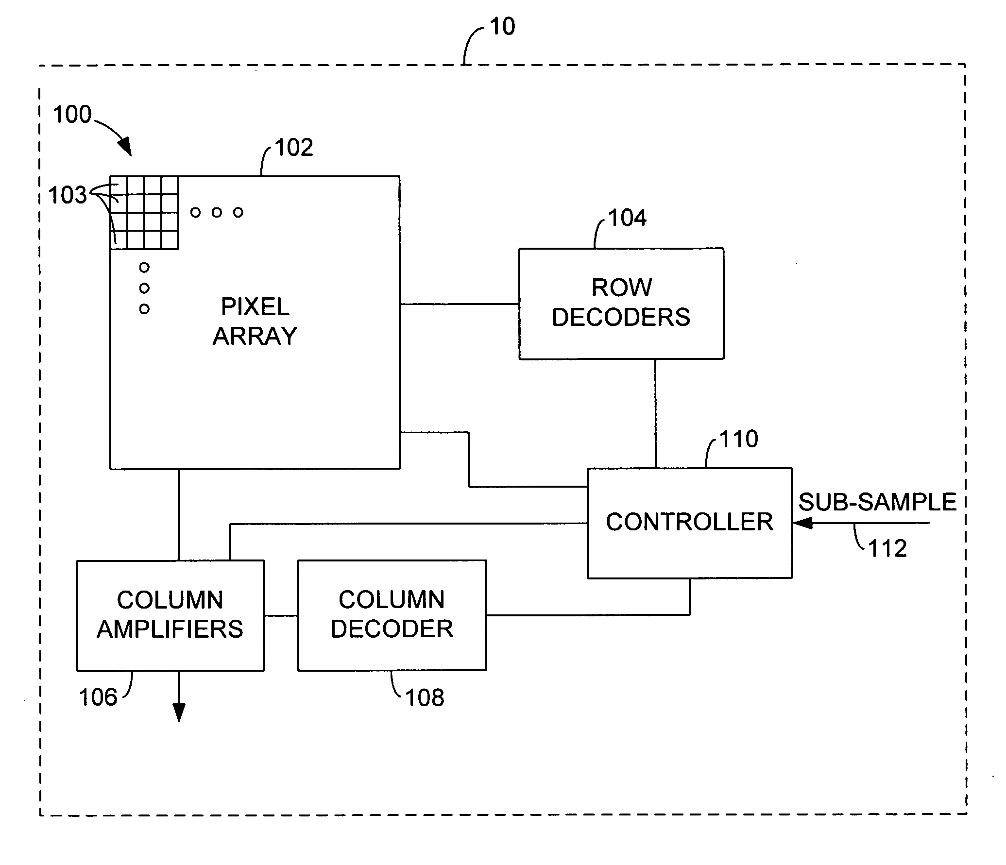
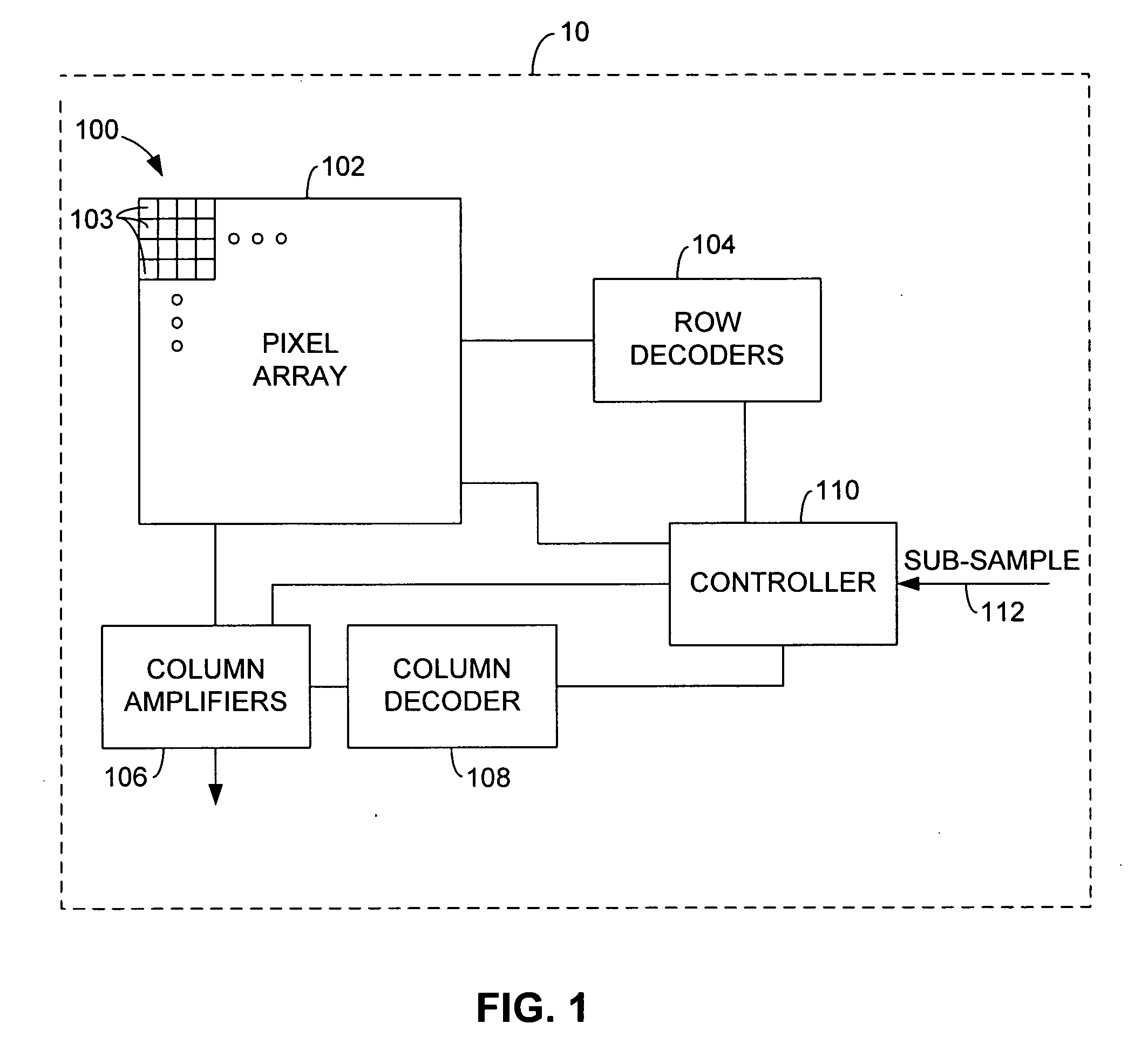
[0011]FIG. 1 is a block diagram illustrating major components of an active pixel sensor (APS) image sensor 100 according to one embodiment of the present invention. Sensor 100 is formed on an integrated circuit 10 and includes pixel array 102, row decoders 104, column amplifiers 106, column decoder 108, and controller 110. Pixel array 102 includes a plurality of pixel circuits (pixels) 103, with each pixel cir...


PUM


Abstract

An active pixel sensor (APS) image sensor comprises an array of pixel circuits corresponding to rows and columns of pixels, a plurality of amplifiers that buffer signals output by the array of pixel circuits, and a plurality of sample and hold circuits that read the buffered signals. A routing mechanism is positioned between the array of pixel circuits and the plurality of amplifiers. A controller selects a set of the pixel circuits for sampling and is configured to control the routing mechanism to couple each pixel circuit in the set to a different one of the amplifiers during a normal mode of operation and to couple each pixel circuit of a subset of pixel circuits in a first set of pixel circuits to a different amplifier of a first subset of the amplifiers, to couple each pixel circuit of a subset of pixel circuits in a second set of pixel circuits to a different amplifier of a second subset of the amplifiers, and to connect the amplifiers of the first and second subsets of amplifiers in pairs to a common one of the sample and hold circuits during a sub-sampling mode of operation.

Description

BACKGROUND OF THE INVENTION [0001] One type of prior art image sensor is a charge-coupled device (CCD) image sensor. CCD image sensors typically include a very closely packed array of polysilicon electrodes that are formed on the surface of the CCD imaging chip. Conceptually, a CCD is a two-dimensional array of Metal Oxide Semiconductor (MOS) capacitors that collect and transfer photon-generated charge. CCD image sensors typically include multiple shift registers to transfer charge from the CCD array to amplifiers. [0002] Another type of prior art image sensor is an active pixel sensor (APS) image sensor. APS image sensors are typically fabricated using Complimentary Metal Oxide Silicon (CMOS) processing technology, and are also typically referred to as CMOS image sensors. APS image sensors sense light by converting incident light (photons) into electronic charge (electrons) by a photo-conversion process. Color APS image sensors are typically made by coating each individual pixel wi...

Claims


Application Information

Patent Timeline
Patent Type & Authority Applications(United States)
IPC IPC(8): H01L27/00
CPCH04N3/1512H04N9/045H04N3/1562H04N25/76H04N25/75
Inventor MENTZER, RAY ALLENDEMONTE, FRANK J.BECK, JEFFERY STEVENBORG, MATTHEW MICHAELMYERS, CHARLES GRANT
Owner APTINA IMAGING CORP
Why Eureka
Try Eureka