Plasma display device

a display device and plasma technology, applied in the direction of static indicating devices, instruments, etc., can solve the problems of deteriorating picture quality, hindering the correct write operation, writing discharge, etc., to minimize the change in black level, prevent the effect of deterioration of contras

Inactive Publication Date: 2007-11-01
PANASONIC CORP
View PDF6 Cites 2 Cited by
  • Summary
  • Abstract
  • Description
  • Claims
  • Application Information

AI Technical Summary

Benefits of technology

[0015] This makes it possible to minimize changes in the black level due to initialization discharge in response to continuously changing signals. Accordingly, deterioration of contrast is preventable and the display screen flicker can be minimized.
[0016] With the present invention, the write operation can be correctly executed in all discharge cells without degrading the contrast even if discharge interference occurs between adjacent cells or a subfield with small weight is disposed far timewise from the initialization period.
[0017] Different voltages of initialization waveforms are determined depending on the level of input picture signal, and the present invention includes the initialization voltage determination unit for determining the voltage of initialization waveform in proportion to the level of input picture signal. This enables minimization of changes in the black level due to initialization discharge in response to continuously changing signals. Accordingly, the present invention prevents deterioration of contrast and also minimizes the display screen flicker.

Problems solved by technology

However, there are many factors that significantly delay a write discharge: No high voltage is applicable to the write pulse due to restrictions of the circuit configuration, the phosphor layer formed on the data electrodes hinders discharge, and so on.
This hinders a correct write operation, and the predetermined discharge cell becomes a dark spot, notably deteriorating picture quality.
This discharge cell with weakened wall charge as described above cannot recover its correct write and luminescence sustain operations until one entire field is completed, and this causes deterioration of picture quality.

Method used


Image

  • Plasma display device
  • Plasma display device
  • Plasma display device

Examples


Embodiment Construction

Exemplary Embodiment

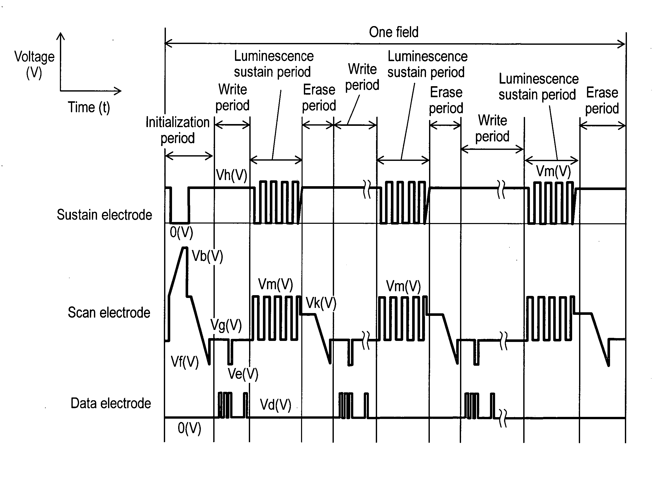
[0034] A plasma display device in an exemplary embodiment of the present invention is described below with reference to FIGS. 1 to 5.

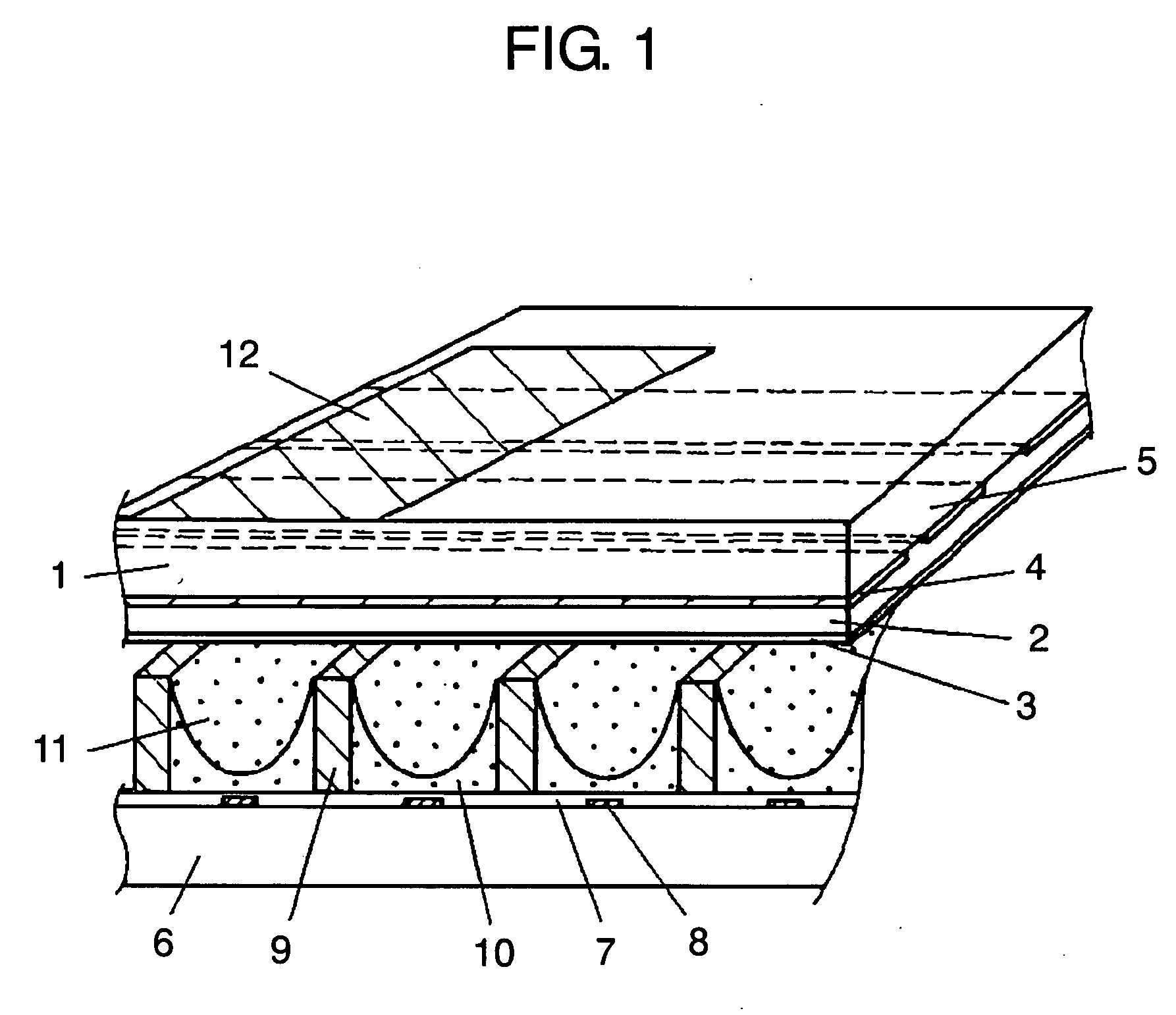
[0035] First, a panel structure is described with reference to FIG. 1. As shown in FIG. 1, a pair of scan electrode 4 and sustain electrode 5 are disposed in parallel on first glass substrate 1, and covered with dielectric layer 2 and protective layer 3. Data electrodes 8 are disposed on second glass substrate 6, and covered with insulating layer 7. Barrier ribs 9 are disposed on insulating layer 7 between data electrodes 8 in a way such that barrier ribs 9 are parallel to data electrodes 8. Phosphor 10 is provided on the surface of insulating layer 7 and a side face of barrier ribs 9. First glass substrate 1 and second glass substrate 6 are disposed facing each other with discharge space 11 in between in a way such that scan electrode 4 and sustain electrode 5 are orthogonal to data electrodes 8. Discharge gas is filled in discha...


PUM


Abstract

Initialization waveforms with different voltages are applied respectively to a predetermined subfield with a small number of sustain pulses, and a subfield with the smallest number of sustain pulses in subfields other than the predetermined subfield. This offers a plasma display device that achieves a correct write operation in all discharge cells even if discharge interference occurs between adjacent cells, and also achieves a high contrast.

Description

TECHNICAL FIELD [0001] The present invention relates to plasma display devices for displaying images by controlling discharge. BACKGROUND ART [0002] In a surface-discharge AC panel, which is a typical plasma display panel (hereafter “panel”), numerous discharge cells are formed between a front panel and rear panel facing each other. In the front panel, display electrodes, respectively consisting of a pair of scan electrode and sustain electrode, are disposed parallel to each other on a front glass substrate, and they are covered with a dielectric layer and a protective layer. In the rear panel, data electrodes are disposed parallel to each other on a rear glass substrate, and they are covered with a dielectric layer. Barrier ribs are formed parallel to data electrodes, and a phosphor layer is formed on the surface of the dielectric layer and a side face of the barrier ribs. Then, the front panel and the rear panel are disposed facing each other in a way such that the display electro...

Claims


Application Information

Patent Timeline
Patent Type & Authority Applications(United States)
IPC IPC(8): G09G3/28G09G3/292G09G3/20G09G3/288G09G3/291G09G3/293G09G3/294G09G3/298
CPCG09G3/2022G09G3/2927G09G2360/16G09G2320/0238G09G2320/0219G09G3/291G09G3/296
Inventor TAKEDA, MINORU
Owner PANASONIC CORP
Why Eureka
Try Eureka