Electro-optical device and electronic apparatus including the same

a technology of optical devices and electronic devices, applied in the field of optical devices, can solve the problems of low thermal conductivity of inorganic alignment layers, degradation of electro-optical materials, and increased temperature of electro-optical devices, and achieve the effect of efficient dissipation of heat of electro-optical materials

Inactive Publication Date: 2009-03-26
SEIKO EPSON CORP
View PDF8 Cites 11 Cited by
  • Summary
  • Abstract
  • Description
  • Claims
  • Application Information

AI Technical Summary

Benefits of technology

[0006]An advantage of some aspects of the invention is that it provides an electro-optical device which can efficiently dissipate the heat of an electro-optical material so that the properties of the electro-optical material can be prevented from being degraded, and an electronic apparatus including the electro-optical device.

Problems solved by technology

When such an electro-optical device is used, for example, in an electronic apparatus provided with a strong light source, such as a projector, there is a possibility that the temperature of the electro-optical device is increased by the radiant heat of the light source or the like, resulting in degradation of the properties of an electro-optical material, such as a liquid crystal.
However, when a liquid crystal device, which is an example of an electro-optical device, includes an inorganic alignment layer, an inorganic material constituting the inorganic alignment layer has low thermal conductivity.
In such a case, even if the technique described in Patent Document 1 or 2 is used, the heat of its liquid crystal layer is not dissipated sufficiently, which is a technical problem to be solved.
That is, even if the heat-dissipating members are provided outside the pair of substrates, it is difficult to efficiently dissipate the heat of the electro-optical material located in the middle of the electro-optical device in the deposition direction.
In addition, the thermal conductivity of the inorganic material constituting the inorganic alignment layer is low, and thus the heat of the electro-optical material is not easily transferred to the substrates, the heat-dissipating members, etc.

Method used


Image

  • Electro-optical device and electronic apparatus including the same
  • Electro-optical device and electronic apparatus including the same
  • Electro-optical device and electronic apparatus including the same

Examples


first embodiment

[0046]An electro-optical device according to a first embodiment of the invention will be described with reference to FIGS. 1 to 7. In the drawings, in order to make the individual layers and components recognizable, different scales are used for the individual layers and components.

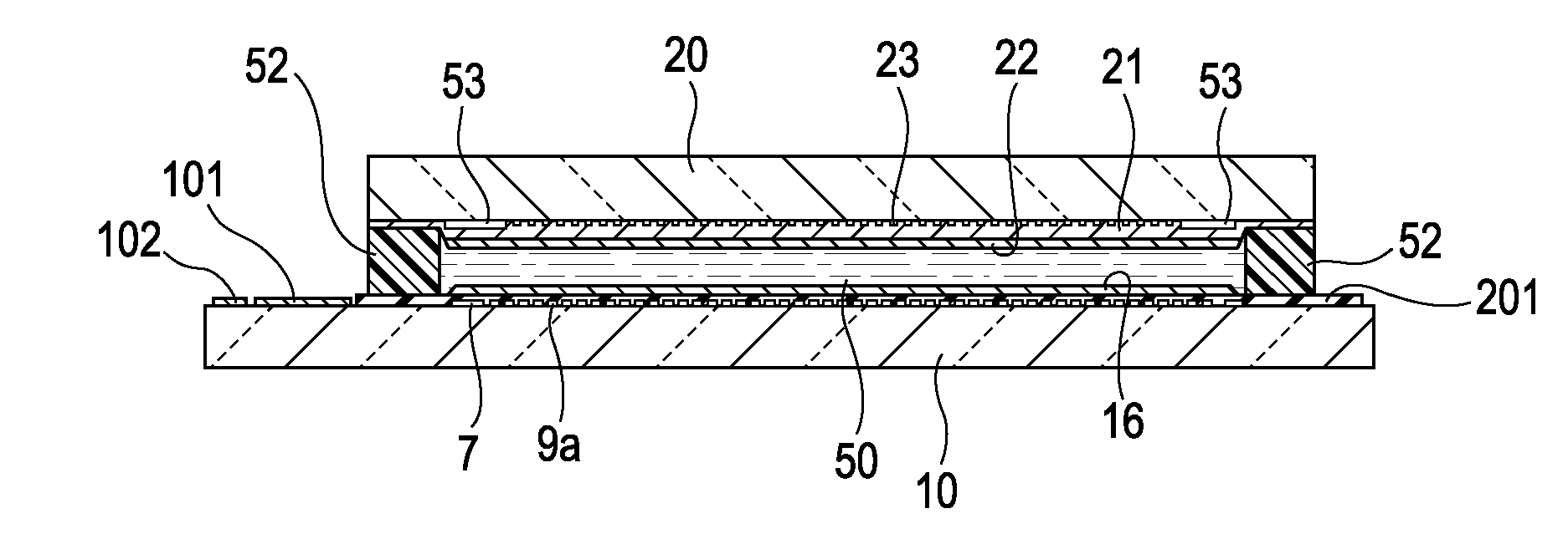
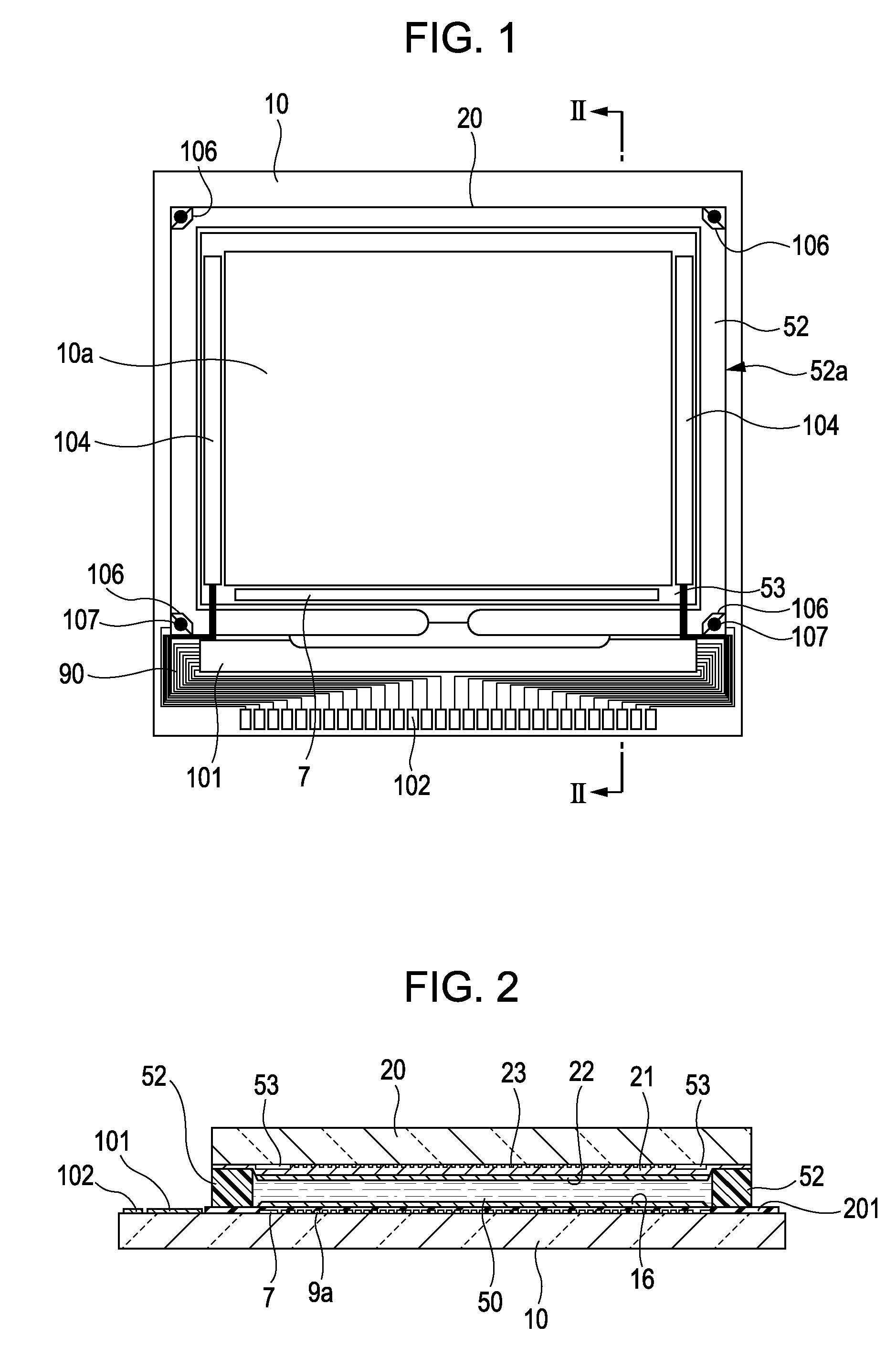
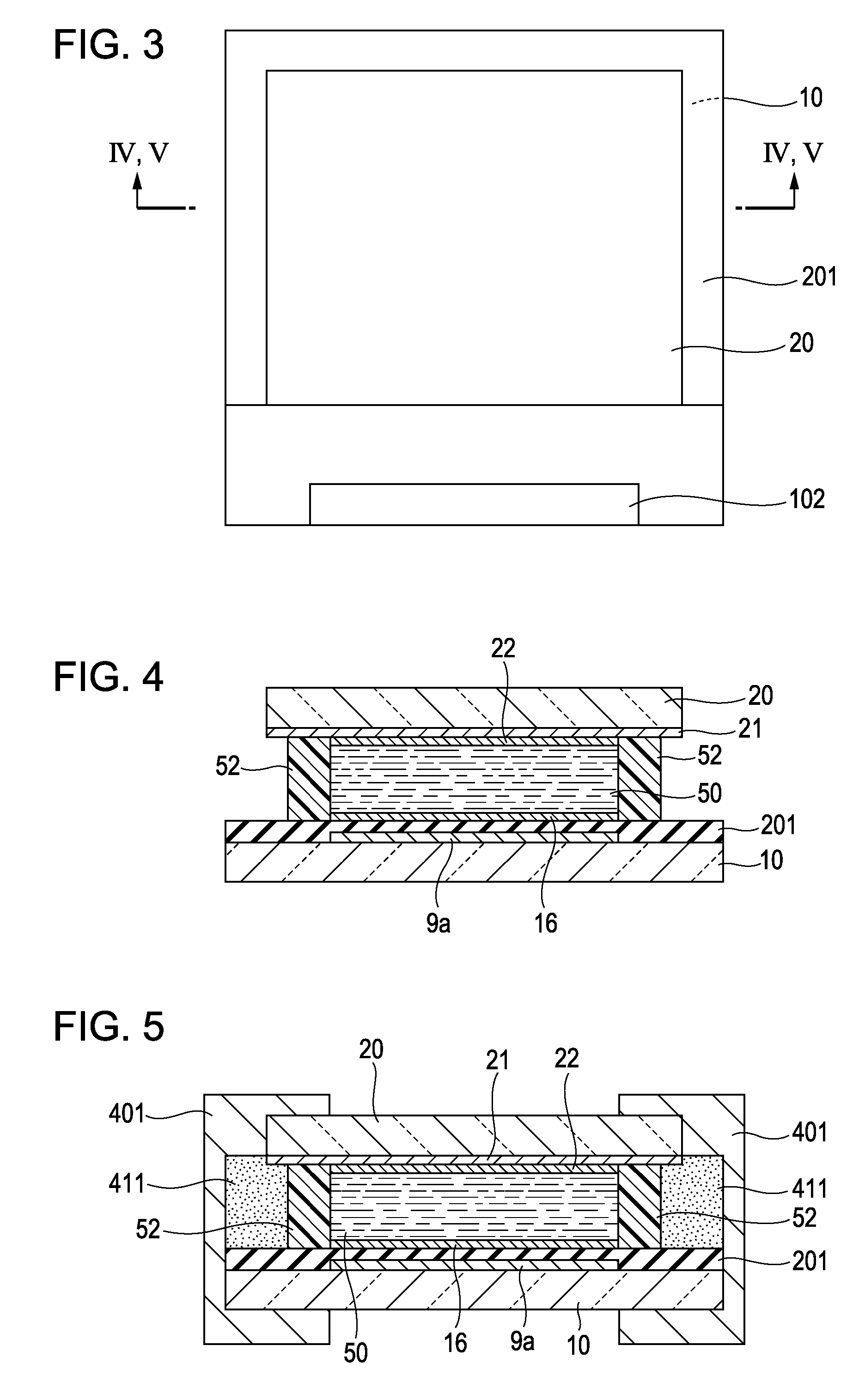
[0047]First, an overall structure of a liquid crystal device according to this embodiment will be described with reference to FIGS. 1 and 2. FIG. 1 is a plan view showing a TFT array substrate together with the individual components disposed thereon, viewed from the counter substrate side, and FIG. 2 is a cross-sectional view taken along the line II-II of FIG. 1. To facilitate explanation, the planar positional relationship between the individual components disposed on the substrate is partially different between FIGS. 1 and 2.

[0048]Referring to FIGS. 1 and 2, in the liquid crystal device according to this embodiment, as an example of a pair of substrates, a TFT array substrate 10 and a counter substrate ...

second embodiment

[0067]An electro-optical device according to a second embodiment of the invention will be described with reference to FIGS. 8 and 9. FIG. 8, which corresponds to FIG. 3, is a plan view showing a liquid crystal device according to this embodiment, viewed from the counter substrate side, and FIG. 9 is a cross-sectional view taken along the line IX-IX of FIG. 8. The second embodiment has the same structure as the first embodiment except that a heat-dissipating layer is disposed on a counter substrate. Consequently, in the second embodiment, duplicate descriptions will be omitted, and the same components or parts as those of the first embodiment are designated by the same reference numerals. Basically, only differences will be described with reference to FIGS. 8 and 9.

[0068]As shown in FIG. 9, a heat-dissipating layer 202 is disposed on a counter electrode 21 disposed on a counter substrate 20. An inorganic alignment layer 22 is disposed on the heat-dissipating layer 202. Some parts of ...

third embodiment

[0069]An electro-optical device according to a third embodiment of the invention will be described with reference to FIGS. 10 and 11. FIG. 10, which corresponds to FIG. 3, is a plan view showing a liquid crystal device according to this embodiment, viewed from the counter substrate side, and FIG. 11 is a cross-sectional view taken along the line XI-XI of FIG. 10. The third embodiment has the same structure as the first embodiment except that heat-dissipating layers are disposed on a TFT array substrate and a counter substrate. Consequently, in the third embodiment, duplicate descriptions will be omitted, and the same components or parts are designated by the same reference numerals. Basically, only differences will be described with reference to FIGS. 10 and 11.

[0070]As shown in FIG. 11, a heat-dissipating layer 203 is disposed on a TFT array substrate 10 so as to cover pixel electrodes 9a. An inorganic alignment layer 16 is disposed on the heat-dissipating layer 203. On the other h...


PUM

PropertyMeasurementUnit
angleaaaaaaaaaa
angleaaaaaaaaaa
temperatureaaaaaaaaaa

Abstract

An electro-optical device includes a pair of substrates, an electro-optical material sandwiched between the pair of substrates, an electrode on one of the pair of substrates, an inorganic alignment layer disposed on the one of the pair of substrates, and a heat-dissipating layer disposed between the electrode and the inorganic alignment layer on the one of the pair of substrates.

Description

BACKGROUND[0001]1. Technical Field[0002]The present invention relates to an electro-optical device, such as a liquid crystal device, and an electronic apparatus, such as a liquid crystal projector, which includes the electro-optical device.[0003]2. Related Art[0004]When such an electro-optical device is used, for example, in an electronic apparatus provided with a strong light source, such as a projector, there is a possibility that the temperature of the electro-optical device is increased by the radiant heat of the light source or the like, resulting in degradation of the properties of an electro-optical material, such as a liquid crystal. Consequently, techniques have been proposed in which heat dissipation is improved by using a transmissive oxide crystal body, such as magnesium oxide (MgO) or yttrium oxide (Y2O3) , or a fluoride single crystal, such as calcium fluoride (CaF2), magnesium fluoride (MgF2), or barium fluoride (BaF2) , as a dustproof substrate in a liquid crystal di...

Claims


Application Information

Patent Timeline
Patent Type & Authority Applications(United States)
IPC IPC(8): G02F1/1337G02F1/1333
CPCG02F1/133382H04N9/3144G02F1/133734
Inventor TANAKA, TAKAAKI
Owner SEIKO EPSON CORP
Why Eureka
Try Eureka