Printed circuit board and method for manufacturing the same

Active Publication Date: 2013-06-13
SAMSUNG ELECTRO MECHANICS CO LTD
View PDF2 Cites 16 Cited by
  • Summary
  • Abstract
  • Description
  • Claims
  • Application Information

AI Technical Summary

Benefits of technology

[0013]It is another object of the present invention to provide a printed circuit board capable of reducing a height of a via in correspondence to a size of the via by employing a structure in which a portion of a pad electrically connected to the via is embedded in an insulator and a circuit pattern is not embedded i

Problems solved by technology

However, in order to respond to a demand for high density and thinning of a printed circuit board, high-density interlayer connection and a fine circuit should be implemented by reducing the size of the pad and the via formed under the pad, but when forming a printed circuit board according to the prior art, there is a limitation in reducing the size of the via.
That is, when simply reducing the size of the via, there is a difficulty in completely plating the v

Method used


Image

  • Printed circuit board and method for manufacturing the same
  • Printed circuit board and method for manufacturing the same
  • Printed circuit board and method for manufacturing the same

Examples


Embodiment Construction

[0049]The terms or words used in the present specification and claims should not be interpreted as being limited to typical or dictionary meanings, but should be interpreted as having meanings and concepts relevant to the technical spirit of the present invention based on the rule according to which an inventor can appropriately define the concept of the term to describe his / her own invention in the best manner.

[0050]Therefore, configurations shown in embodiments and the drawings of the present invention rather are examples of the most exemplary embodiment and do not represent all of the technical spirit of the invention. Thus, it will be understood that various equivalents and modifications that replace the configurations are possible when filing the present application.

[0051]Hereinafter, embodiments of the present invention will be described in detail with reference to the accompanying drawings.

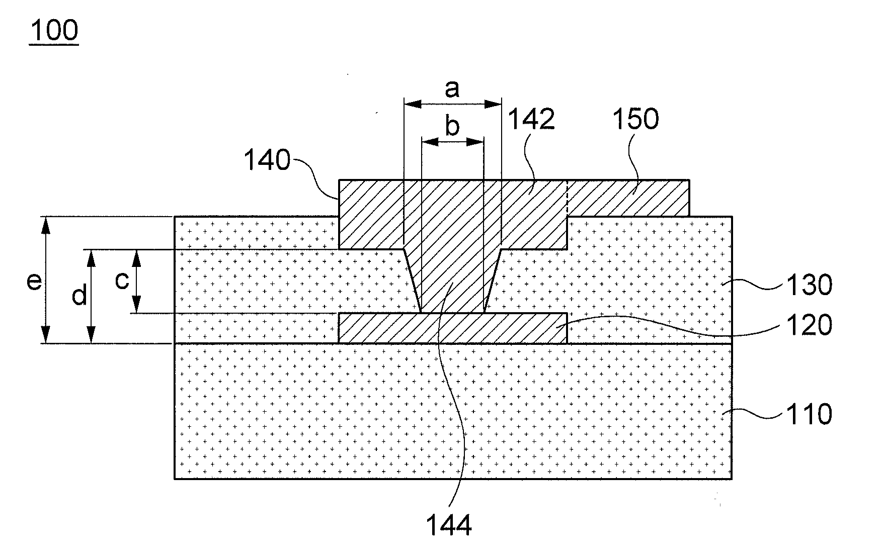
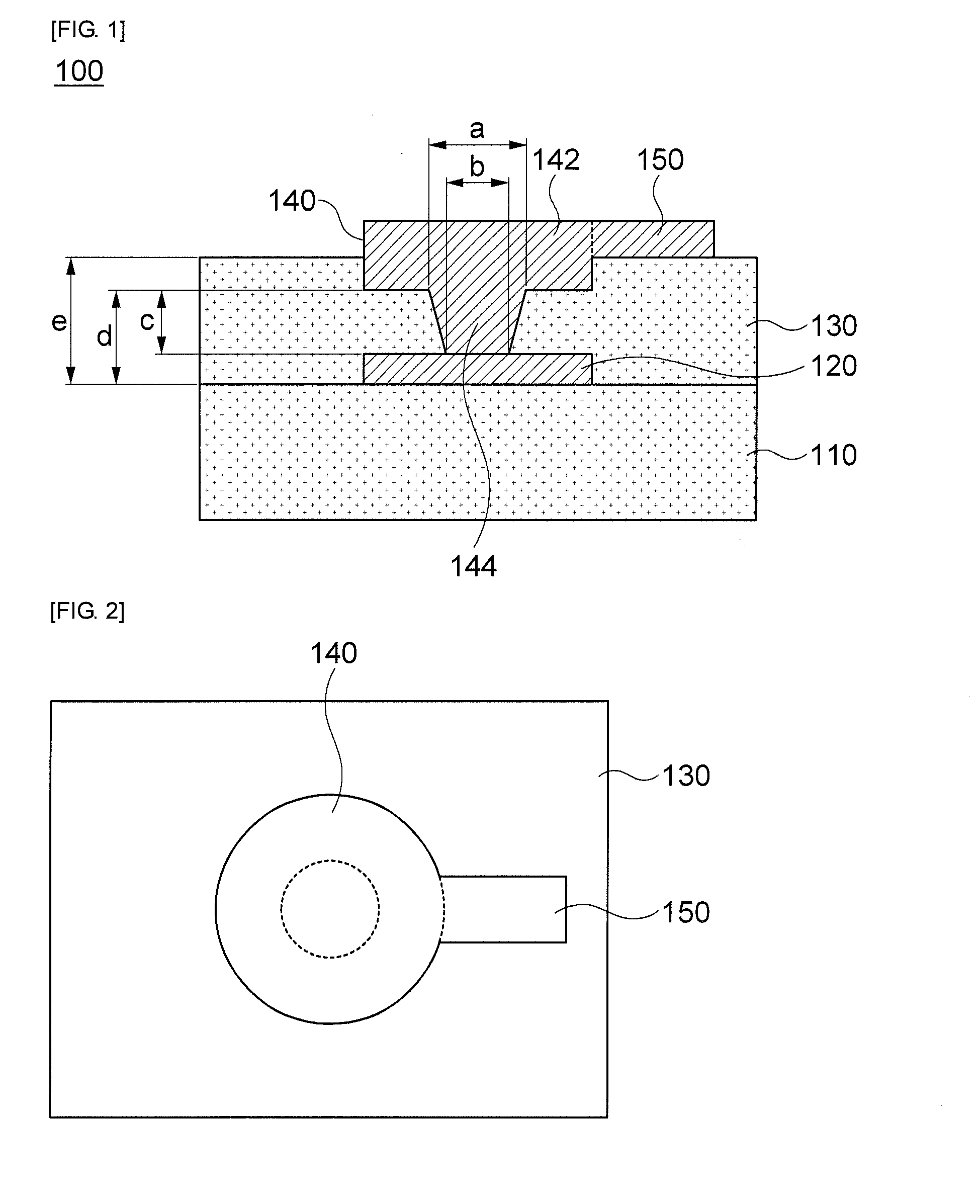
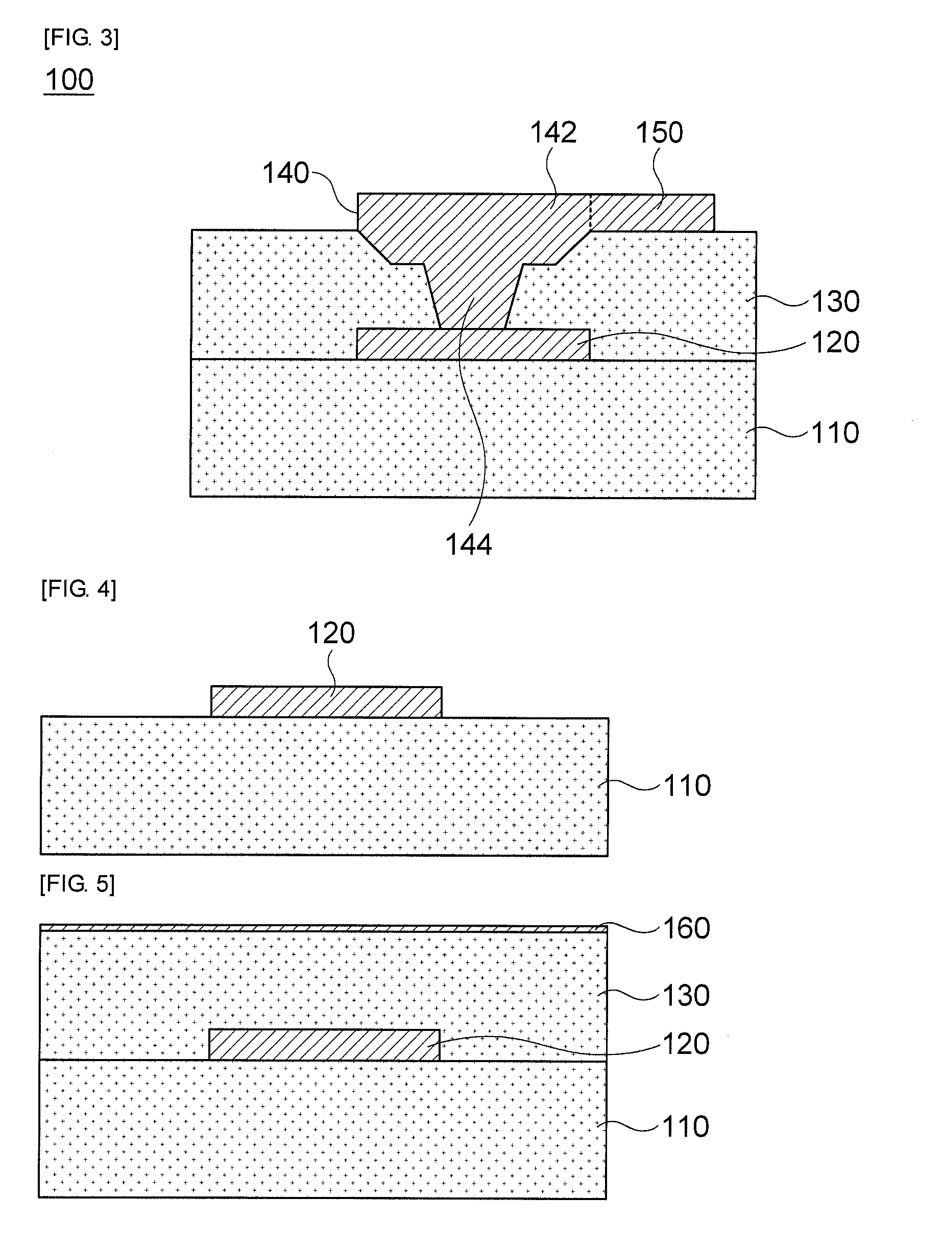
[0052]FIG. 1 is a cross-sectional view of a printed circuit board in accordance with an...


PUM

PropertyMeasurementUnit
Thicknessaaaaaaaaaa
Diameteraaaaaaaaaa
Areaaaaaaaaaaa

Abstract

The present invention relates to a printed circuit board including: a first circuit pattern formed on a first insulator; a second insulator formed on the first insulator; a second circuit pattern having a pad of which a portion is embedded in the second insulator and a via which penetrates the second insulator to electrically connect the first circuit pattern and the pad; and a third circuit pattern formed on the second insulator, and it is possible to reduce a size of the via without increasing an aspect ratio.

Description

CROSS-REFERENCE TO RELATED APPLICATIONS[0001]Claim and incorporate by reference domestic priority application and foreign priority application as follows:Cross Reference to Related Application[0002]This application claims the benefit under 35 U.S.C. Section 119 of Korean Patent Application Serial No. 10-2011-0130378, entitled filed Dec. 7, 2011, which is hereby incorporated by reference in its entirety into this application.BACKGROUND OF THE INVENTION[0003]1. Field of the Invention[0004]The present invention relates to a printed circuit board and a method for manufacturing the same, and more particularly, to a printed circuit board capable of implementing high-density interlayer connection and a fine circuit by reducing a size of a via, and a method for manufacturing the same.[0005]2. Description of the Related Art[0006]In recent times, miniaturization and technology integration of electronic devices and products have been steadily developed due to advance of the electronic devices ...

Claims


Application Information

Patent Timeline
IPC IPC(8): H05K1/11H05K3/36
CPCH05K1/115H05K3/0035Y10T29/49126H05K2203/1476H05K2201/09845H05K3/40H05K3/46
Inventor LEE, HAN UL
Owner SAMSUNG ELECTRO MECHANICS CO LTD
Why Eureka
Try Eureka