Display substrate and method of manufacturing the same

a technology of display substrate and substrate, which is applied in the testing/measurement of individual semiconductor devices, semiconductor/solid-state devices, instruments, etc., can solve the problems of non-uniformity of illumination, damage to organic layers or electrodes of organic light-emitting display devices, and increase power consumption, so as to prevent or reduce voltage drop

Active Publication Date: 2014-08-21
SAMSUNG DISPLAY CO LTD
View PDF5 Cites 37 Cited by
  • Summary
  • Abstract
  • Description
  • Claims
  • Application Information

AI Technical Summary

Benefits of technology

[0009]Aspects of embodiments of the present invention are directed toward a display substrate and a method of manufacturing

Problems solved by technology

However, the large display increases a wiring resistance of an electrode that covers all pixels, and the increased wiring resistance causes a voltage drop, resulting in luminance non-uniformi

Method used


Image

  • Display substrate and method of manufacturing the same
  • Display substrate and method of manufacturing the same
  • Display substrate and method of manufacturing the same

Examples


Embodiment Construction

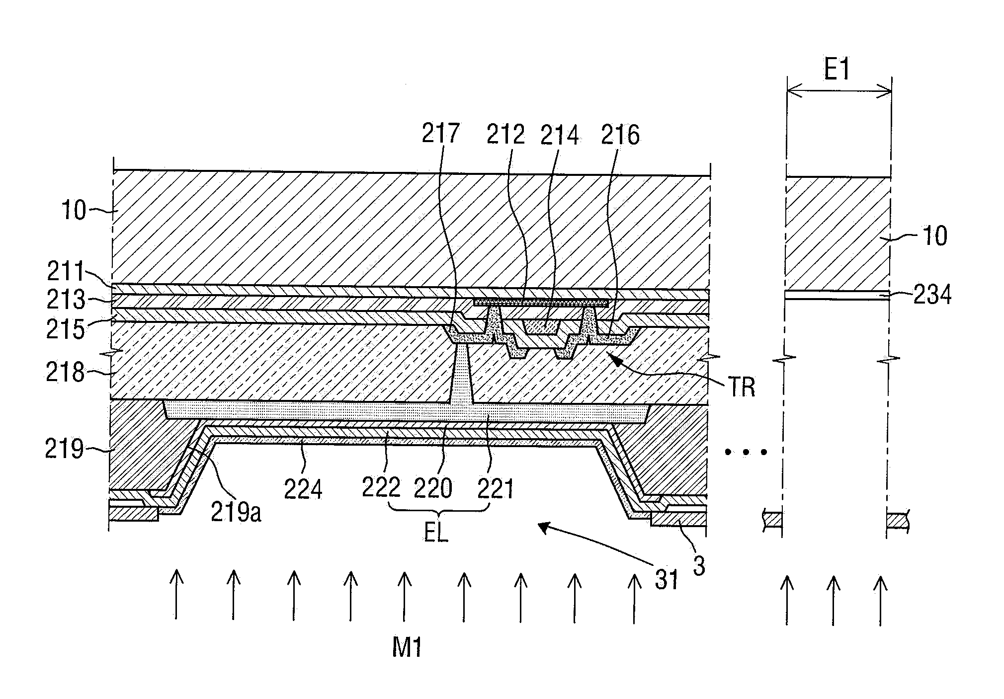
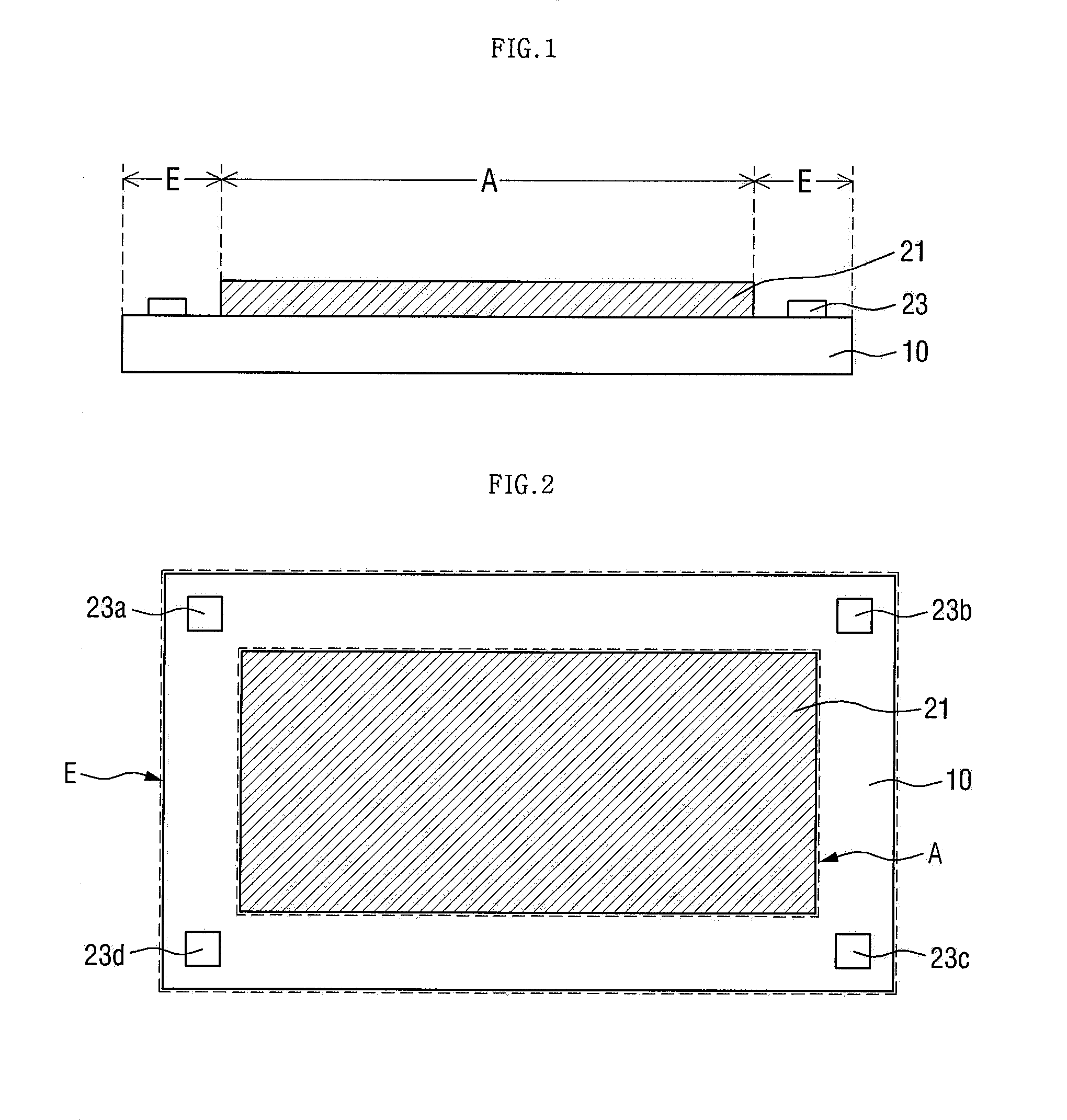
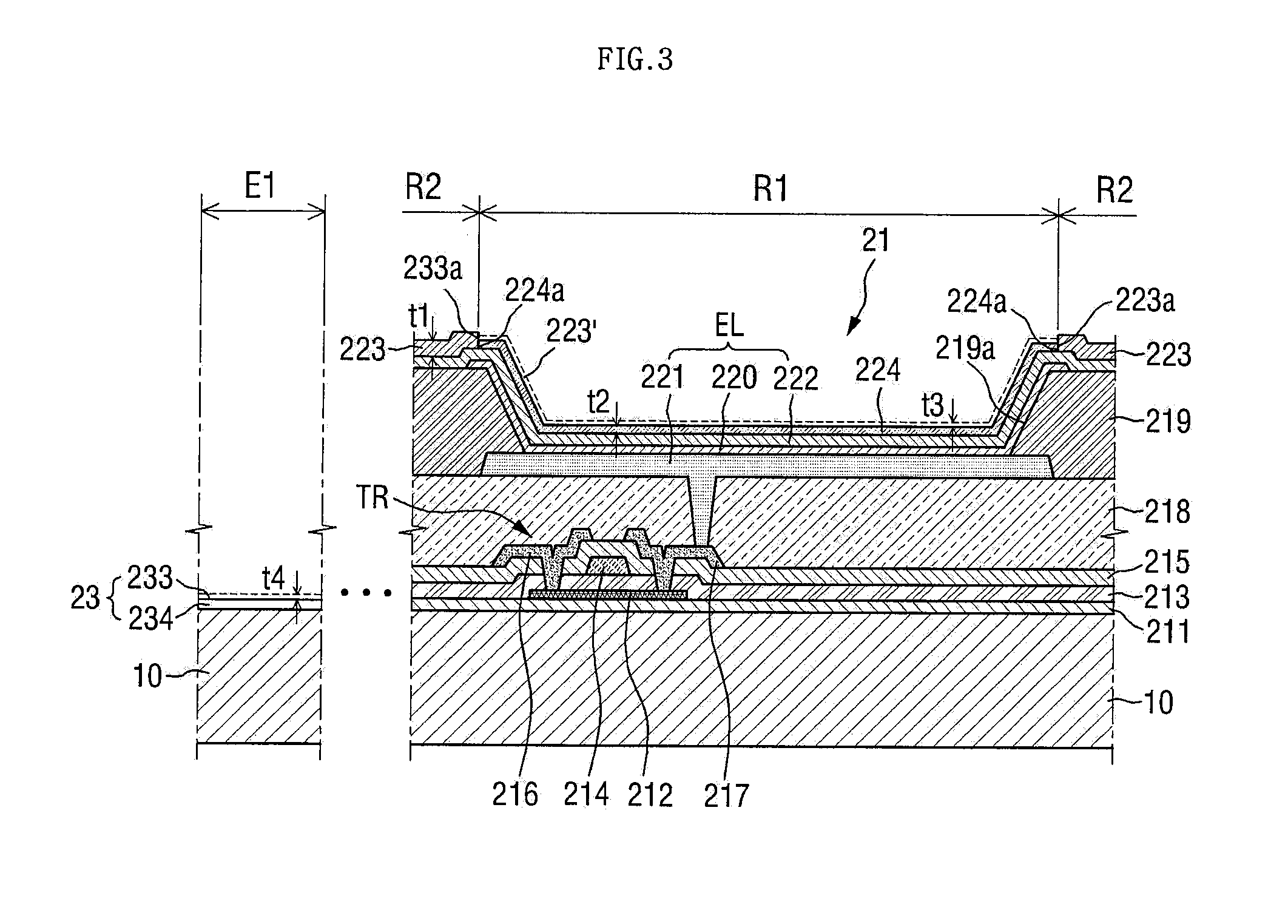
[0057]In the following detailed description, only certain exemplary embodiments of the present invention are shown and described, by way of illustration. As those skilled in the art would recognize, the invention may be embodied in many different forms and should not be construed as being limited to the embodiments set forth herein. Advantages and features of the present invention may be understood more readily by reference to the following detailed description of embodiments and the accompanying drawings. The present invention may, however, be embodied in many different forms and should not be construed as being limited to the embodiments set forth herein. Rather, these embodiments are provided by way of example.

[0058]It will be understood that when an element (e.g. a layer) is referred to as being “on” another element, the element can be directly on the second element, or can be indirectly on the second element, with one or more intervening elements interposed therebetween. Like r...


PUM


Abstract

A display substrate and a method of manufacturing the same. The display substrate includes a substrate including an active area and an inactive area, an organic light-emitting diode (OLED) unit disposed on the active area of the substrate, and a transmittance measurement pattern unit disposed on the inactive area of the substrate. The transmittance measurement pattern unit includes a deposition assistant layer pattern disposed on the substrate.

Description

CROSS-REFERENCE TO RELATED APPLICATION[0001]This application claims priority to and the benefit of Korean Patent Application No. 10-2013-0016422 filed on Feb. 15, 2013 in the Korean Intellectual Property Office, the content of which is incorporated herein by reference in its entirety.BACKGROUND[0002]1. Field[0003]The present invention relates to a display substrate and a method of manufacturing the same.[0004]2. Description of the Related Art[0005]With the development of display technology, display devices are being widely used in portable devices (such as notebook computers, mobile phones and portable media players (PMPs)) as well as display devices for homes (such as TVs and monitors). In particular, the trend toward lighter and thinner display devices is increasing the popularity of liquid crystal display (LCD) devices, organic light-emitting display devices, etc.[0006]An organic light-emitting display device is a self-emissive display device in which a voltage is applied to an a...

Claims


Application Information

Patent Timeline
IPC IPC(8): H01L27/32H01L21/66
CPCH01L22/12H01L27/3241H01L22/30H10K59/12H10K59/1201H05B33/10H05B33/22H05B33/26H10K59/32H10K59/88H10K59/00H10K59/124H10K59/125H10K50/805H10K71/60H10K59/10H10K71/00H10K71/70
Inventor KIM, SEONG MINCHOI, JUN HO
Owner SAMSUNG DISPLAY CO LTD
Why Eureka
Try Eureka