
Organic light emitting display and driving method of inspection circuit of organic light emitting display

a technology of organic light emitting display and inspection circuit, which is applied in static indicating devices, instruments, error detection/correction, etc., can solve the problems of affecting the operation of the inspection circuit. , to achieve the effect of reducing or preventing interference between cells and preventing or reducing a voltage drop

Active Publication Date: 2011-11-08
SAMSUNG DISPLAY CO LTD
View PDF22 Cites 4 Cited by
  • Summary
  • Abstract
  • Description
  • Claims
  • Application Information

AI Technical Summary

Benefits of technology

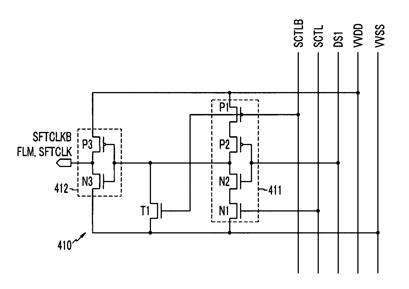
[0009]It is therefore a feature of an embodiment of the present invention to provide an OLED display and a driving method of an inspection circuit of an OLED display for reducing or preventing interference between cells.
[0010]It is therefore another feature of an embodiment of the present invention to provide an OLED display and a driving method of an inspection circuit of an OLED display for preventing or reducing a voltage drop generated during a sheet inspection.

Problems solved by technology

Since such an OLED display may be manufactured through a plurality of manufacturing processes, the manufacturing cost thereof may increase and the reliability may be degraded according to defects caused during the manufacturing processes.
A conventional method of inspecting a sheet having a plurality of cells may generate a defect at a scan line as a result of interference between adjacent cells, and may induce malfunctions of turning on / off adjacent cells because of a voltage drop caused by leakage current.
However, this method cannot measure the power consumption of a scan driver in a sheet unit before scribing.

Method used


Image

  • Organic light emitting display and driving method of inspection circuit of organic light emitting display
  • Organic light emitting display and driving method of inspection circuit of organic light emitting display
  • Organic light emitting display and driving method of inspection circuit of organic light emitting display

Examples


Embodiment Construction

[0031]Korean Patent Application No. 10-2006-0075175 filed on Aug. 9, 2006, in the Korean Intellectual Property Office, and entitled: “Organic Light Emitting Display and Driving Method of Inspector Circuit of Organic Light Emitting Display,” is incorporated by reference herein in its entirety.

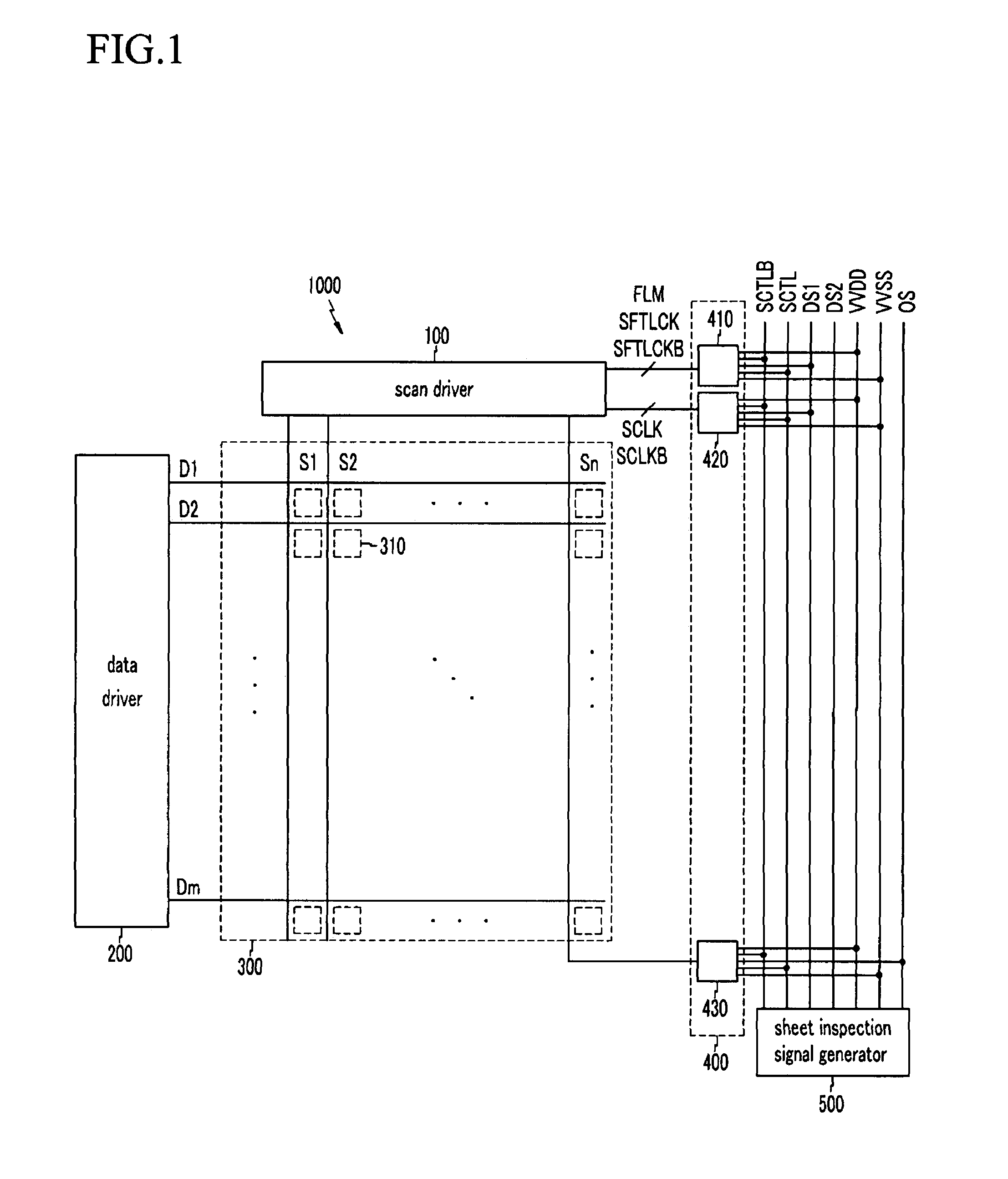
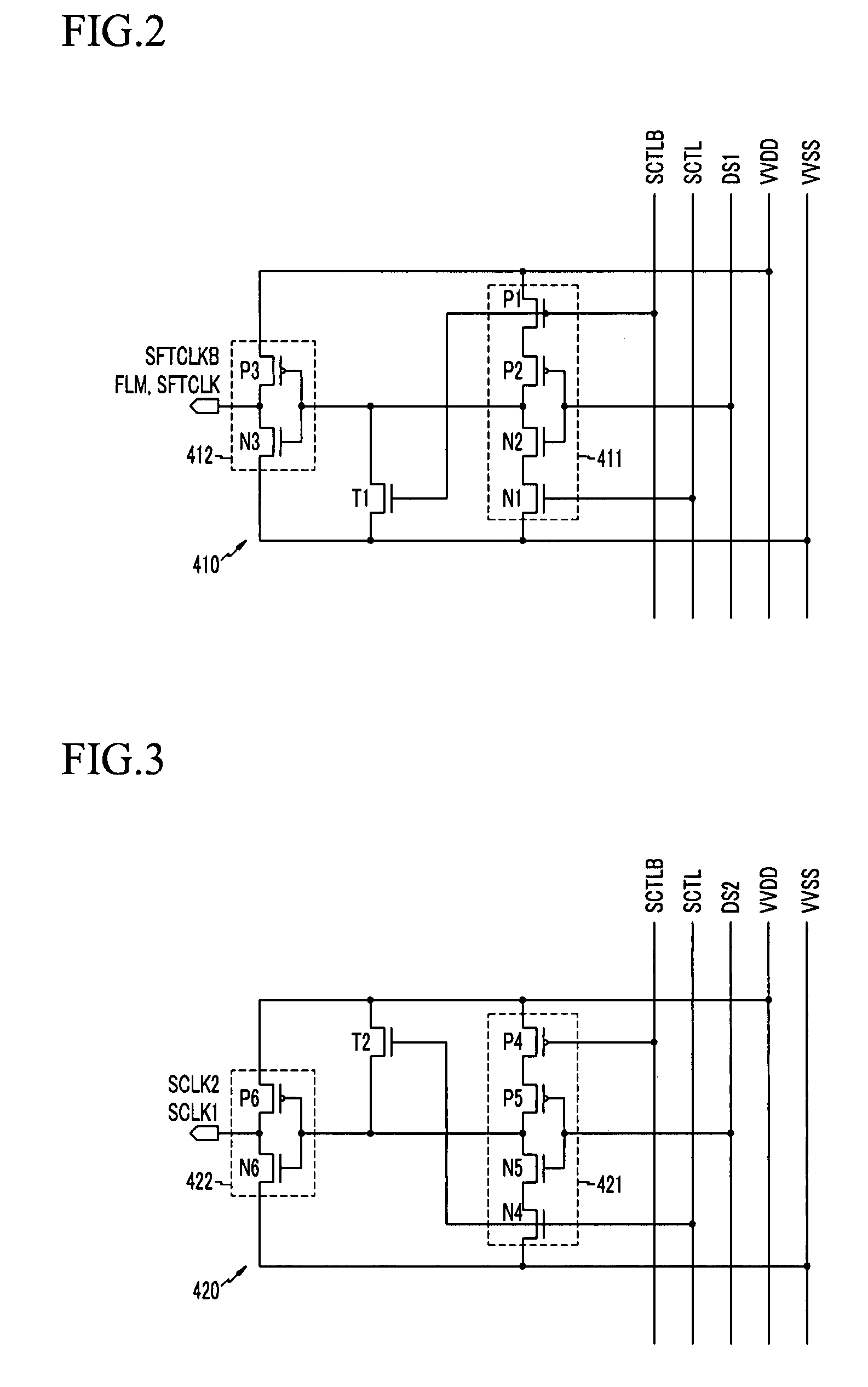
[0032]As will be described in detail below, an organic light emitting diode (OLED) display and a method for driving an inspection circuit of the OLED display according to exemplary embodiments of the present invention are provided, which may reduce or prevent interference between cells and / or a voltage drop while inspecting a sheet including the OLED display.

[0033]In the following detailed description, only certain exemplary embodiments of the present invention have been shown and described, simply by way of illustration. As those skilled in the art would realize, the described embodiments may be modified in various different ways, all without departing from the spirit or scope of the present in...


PUM


Abstract

An OLED display and a driving method of an inspection circuit are provided. The OLED display may include a data driver, a scan driver, a driving transistor, a switching transistor, an organic light emitting diode, and an inspection circuit. The data driver and scan driver may apply a data signal and a scan signal. The driving transistor may generate a current corresponding to a voltage supplied to a first electrode and a control electrode. The switching transistor may apply the data signal to the driving transistor. The organic light emitting diode may be electrically connected to the driving transistor. The inspection circuit may include a three-phase inverter circuit having an input and an output terminal. The input terminal may supply a first power voltage to the output terminal when the output terminal decides an output signal regardless of a signal input to the input terminal.

Description

BACKGROUND OF THE INVENTION[0001]1. Field of the Invention[0002]The present invention relates to an organic light emitting diode (OLED) display, an inspection circuit of an OLED display, and a driving method thereof.[0003]2. Description of the Related Art[0004]With the development of the electronics industry and the increase in the amount of information, there has been much research in active progress for developing a large screen display. Flat panel displays providing a large screen and low power consumption have been introduced to address these issues. Examples thereof include a liquid crystal display (LCD), a plasma display panel (PDP), and an organic light emitting diode (OLED) display. Particularly, OLED displays have been receiving attention as a flat panel display that can be made extremely thin, lightweight and having superior color reproducibility. An OLED display may have various additional advantages, e.g., a faster response speed than an LCD, superior luminance due to it...

Claims


Application Information

Patent Timeline
Patent Type & Authority Patents(United States)
IPC IPC(8): G09G3/32
CPCG09G3/006G09G3/3233G09G2300/0819G09G2300/0842G09G2300/0861G09G2320/043G09G2330/12Y10S345/904G09G3/30G09G3/20G09G3/32G01R19/165
Inventor KWAK, WON-KYUJEONG, JIN-TAE
Owner SAMSUNG DISPLAY CO LTD
Learn More