Data processing device for display device, display device equipped with same and data processing method for display device

a display device and data processing technology, applied in the field of data processing devices for display devices, can solve the problems of inability to achieve the luminance does not reach the desired emission luminance, and the time degradation of the oled has progressed, so as to suppress the degradation of the electro-optical element, reduce the gradation of other pixel circuits, and prevent burn-in

Active Publication Date: 2015-10-01
SHARP KK
View PDF3 Cites 35 Cited by
  • Summary
  • Abstract
  • Description
  • Claims
  • Application Information

AI Technical Summary

Benefits of technology

[0034]According to the first aspect of the present invention, for each pixel circuit based on the equivalent cumulative value of the pixel circuit, a correction coefficient that is approximately equal to or smaller than one is obtained by taking, as a reference, the maximum equivalent cumulative value among the equivalent cumulative values of the plurality of pixel circuits. The equivalent cumulative value of each pixel circuit reflects at least the cumulative value of energy of the current flowing through the electro-optical element (the drive current) included in the pixel circuit. Therefore, the equivalent cumulative value indicates the time degradation of the electro-optical element. Therefore, by using, as corrected gradation data, a product of the correction coefficient obtained as described above and the gradation data, the gradation data is corrected such that gradation of other pixel circuit is lowered, taking as a reference, a pixel circuit having an electro-optical element in which time degradation has progressed most (hereinafter, also referred to as a “pixel circuit in which time degradation has progressed most”). Therefore, the drive current is smaller than an original drive current in other pixel circuit, taking as a reference, a pixel circuit in which time degradation has progressed most. Accordingly, burn-in can be prevented by performing the luminance compensation, while suppressing time degradation of the electro-optical element. Further, since it is not necessary to read various parameters (a voltage applied to both ends of the electro-optical element, a drive current, and the like) from the pixel circuit in order to correct the gradation data in the data processing device, increase in the number of wires can be suppressed.
[0035]According to the second aspect of the present invention, a degradation coefficient indicating time degradation of the electro-optical element in accordance with the

Problems solved by technology

The organic EL display device employing the passive matrix system (hereinafter, referred to as a “passive matrix-type organic EL display device”) has a simple structure, but realization of a large size and high precision is difficult.
That is, when degradation of the OLED has progressed, luminance does not reach desired emission luminance even whe

Method used


Image

  • Data processing device for display device, display device equipped with same and data processing method for display device
  • Data processing device for display device, display device equipped with same and data processing method for display device
  • Data processing device for display device, display device equipped with same and data processing method for display device

Examples


first embodiment

1. First Embodiment

[0068]

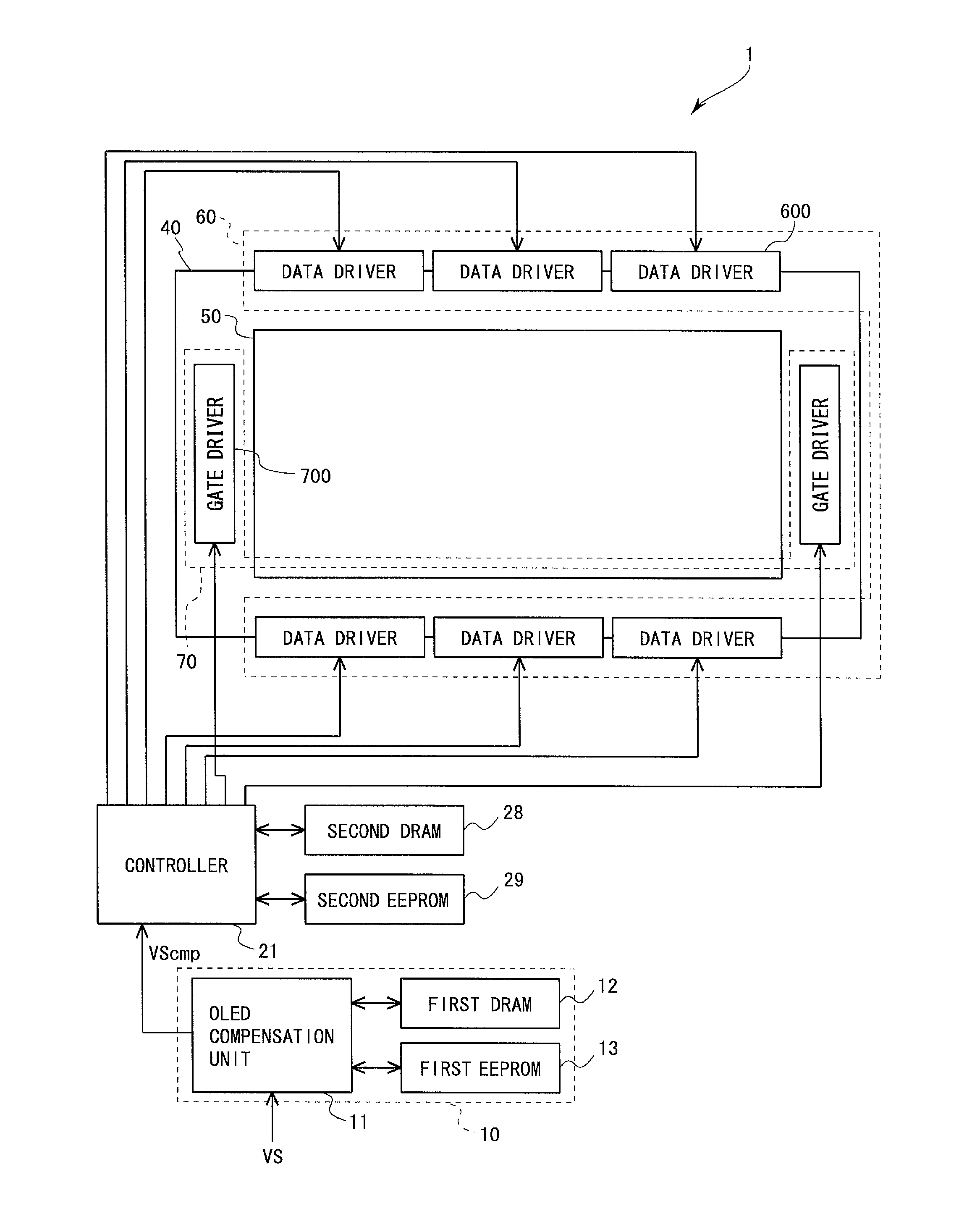
[0069]FIG. 1 is a block diagram showing a configuration of an active matrix-type organic EL display device 1 according to a first embodiment of the present invention. The organic EL display device 1 includes a data processing device 10, a controller 21 as a display control unit, a second dynamic random access memory (DRAM) 28, a second electrically erasable programmable read-only memory (EEPROM) 29, a display panel 40, a data drive unit 60, and a scanning drive unit 70. On the display panel 40, there are arranged the data drive unit 60 and the scanning drive unit 70. One or both of the data drive unit 60 and the scanning drive unit 70 may be integrally formed with the display unit 50. The second DRAM 28 and the second EEPROM may be provided inside the controller 21. The data processing device 10 includes an OLED compensation unit 11, a first DRAM 12, and a first EEPROM 13, and is realized as one chip set.

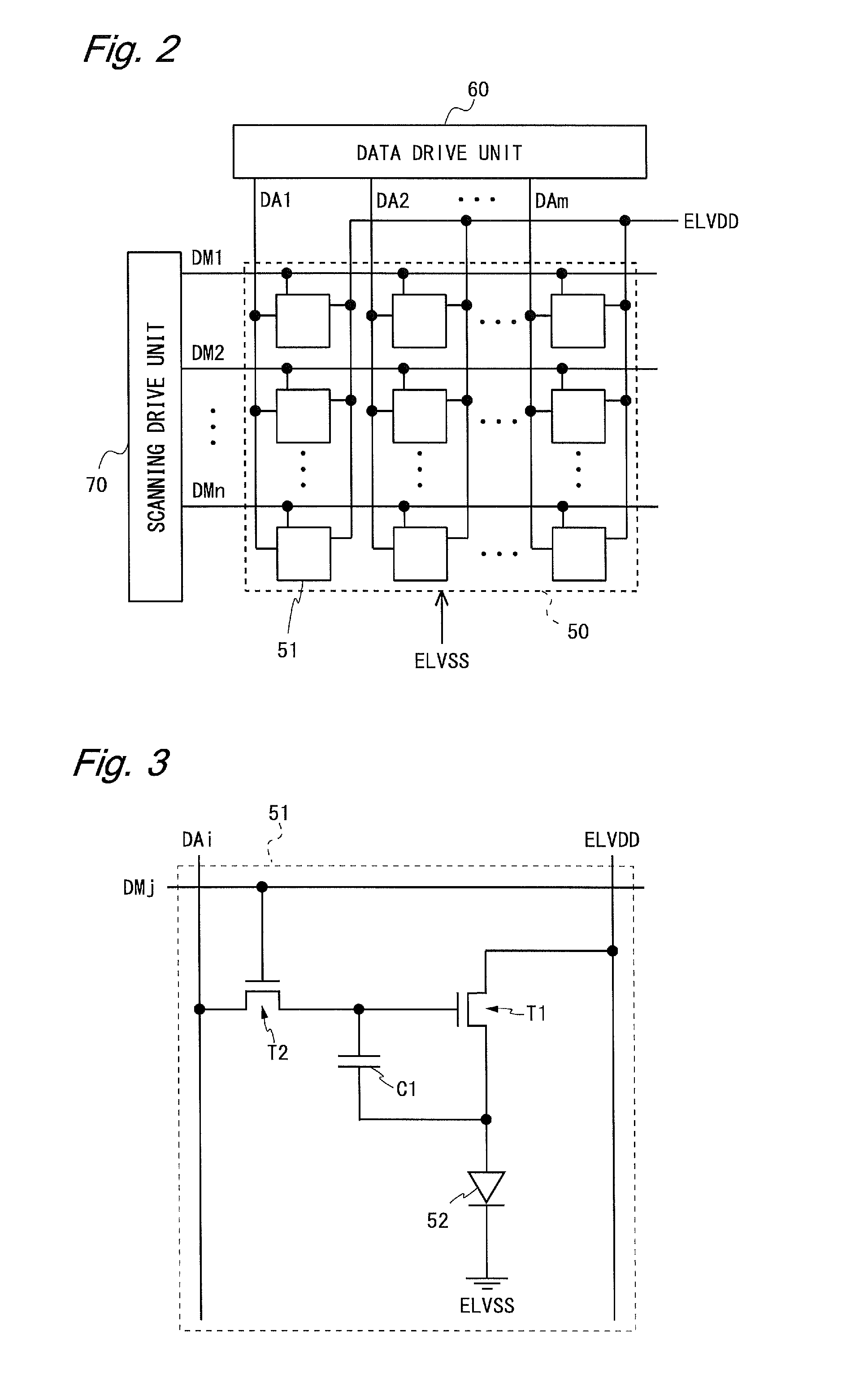
[0070]FIG. 2 is a block diagram for describing a confi...

second embodiment

2.1. Second Embodiment

[0111]

[0112]FIG. 10 is a block diagram showing a configuration of the active matrix-type organic EL display device 1 according to a second embodiment of the present invention. In the constituent elements of the present embodiment, for the elements same as those of the above first embodiment, the same reference characters are attached and the descriptions are omitted appropriately. The controller 21 in the present embodiment includes a TFT compensation unit 200. Each data driver 600 includes a data voltage supplying unit 610 and a current measurement unit 620. The data voltage supplying unit 610 has functions similar to those of the data driver 600 in the above first embodiment. The current measurement unit 620 measures a drive current obtained from the pixel circuit 51 in accordance with a data voltage based on drive gradation data, and acquires measurement data indicating a current value of the drive current. The current measurement unit 620 transmits the acqu...

third embodiment

3. Third Embodiment

[0169]

[0170]FIG. 15 is a block diagram showing a configuration of the active matrix-type organic EL display device 1 according to a third embodiment of the present invention. In the constituent elements of the present embodiment, for the elements same as those of the above first embodiment, the same reference characters are attached and the descriptions are omitted appropriately. In the present embodiment, the TFT compensation unit 200 is provided in the controller 21 in the above first embodiment. The configuration of the pixel circuit 51 may be similar to that in the above first embodiment or similar to that in the above second embodiment.

[0171]The TFT compensation unit 200 in the present embodiment performs various compensations without using the measurement data I, unlike that in the above second embodiment. As contents and techniques of compensation by the TFT compensation unit 200, all known contents and techniques can be employed, including the following, f...


PUM


Abstract

A unit equivalent value acquiring unit acquires a normal-temperature unit equivalent use time Δtn by using a temperature sensor, first to third LUTs, and a first multiplying unit. An integration unit acquires an equivalent cumulative use time to by integrating the normal-temperature unit equivalent use time Δtn. A maximum value detecting unit detects a maximum equivalent cumulative use time tnmax. A dividing unit acquires a correction coefficient Kcmp by dividing total degradation E(tnmax,Tn) acquired by a fourth LUT by total degradation E(tn,Tn) acquired by a fifth LUT. Accordingly, there is provided a data processing device for a display device capable of preventing burn-in while suppressing time degradation of an electro-optical element and increase in the number of wires.

Description

TECHNICAL FIELD[0001]The present invention relates to a data processing device for a display device, and more particularly, relates to a data processing device for a display device using an electro-optical element such as an organic light-emitting diode (OLED) as a display element, a display device equipped with the data processing device, and a data processing method for the display device.BACKGROUND ART[0002]Conventionally, as for a display element provided in a display device, there exist an electro-optical element whose luminance is controlled by an applied voltage and an electro-optical element whose luminance is controlled by a flowing current. A liquid-crystal display element is a representative example of the electro-optical element whose luminance is controlled by an applied voltage. On the other hand, an OLED is a representative example of the electro-optical element whose luminance is controlled by a flowing current. The OLED is also called an organic electro-luminescence...

Claims


Application Information

Patent Timeline
IPC IPC(8): G09G5/10G09G3/32
CPCG09G3/3283G09G5/10G09G3/3233G09G2300/0819G09G2320/045G09G2320/046G09G2320/0295
Inventor OHTA, YOSHIFUMITAKAHAMA, KENGO
Owner SHARP KK
Why Eureka
Try Eureka