
Data processing device for display device, display device equipped with same and data processing method for display device
a display device and data processing technology, applied in static indicating devices, cathode-ray tube indicators, instruments, etc., can solve the problems of inability to achieve a large size and high precision, the luminance does not reach the desired emission luminance, and the time degradation of the oled has progressed, so as to suppress the degradation of the electro-optical element. , the effect of reducing the gradation of other pixel circuits and preventing burn-in
- Summary
- Abstract
- Description
- Claims
- Application Information
AI Technical Summary
Benefits of technology
Problems solved by technology
Method used
Image

Examples
first embodiment
1. First Embodiment
[0069]
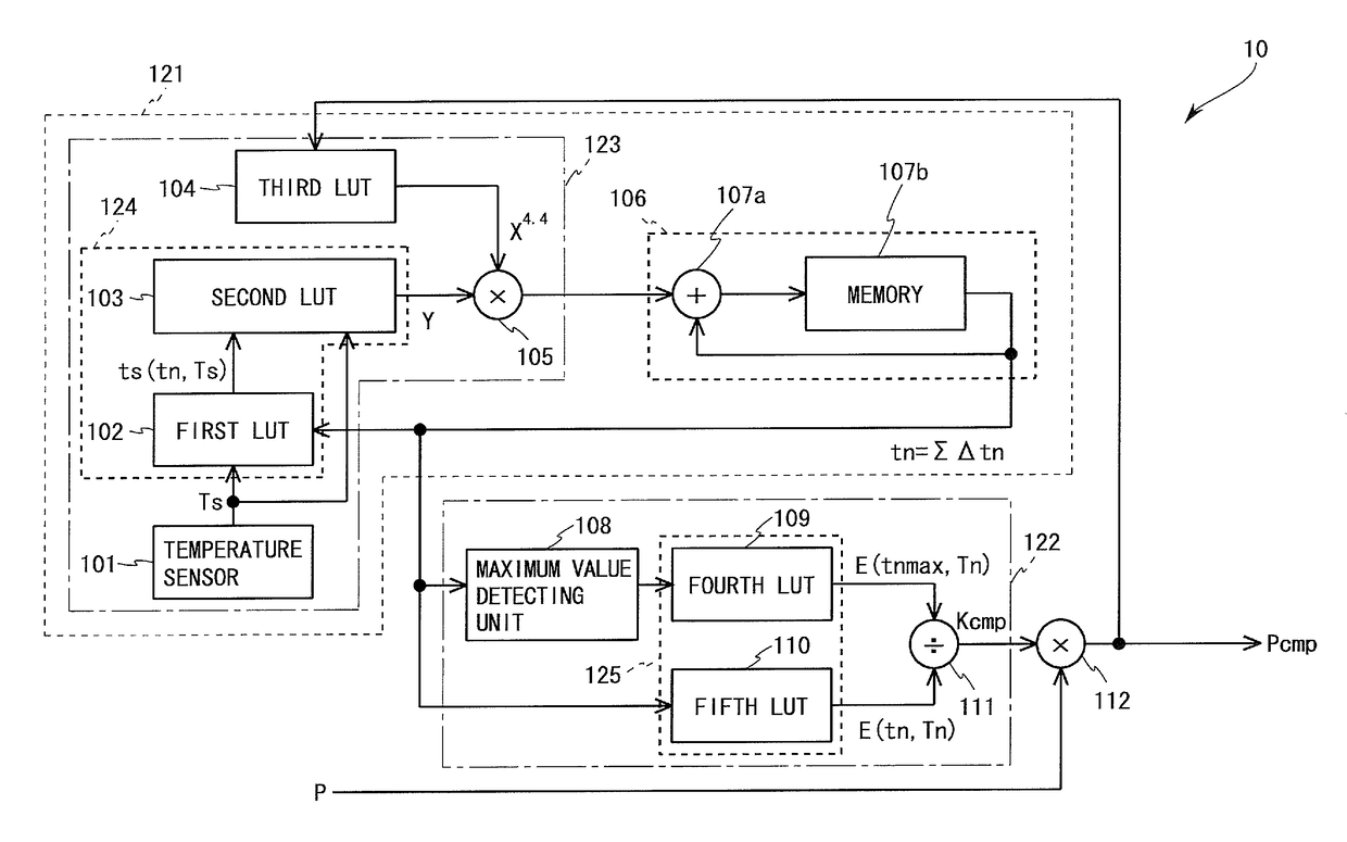
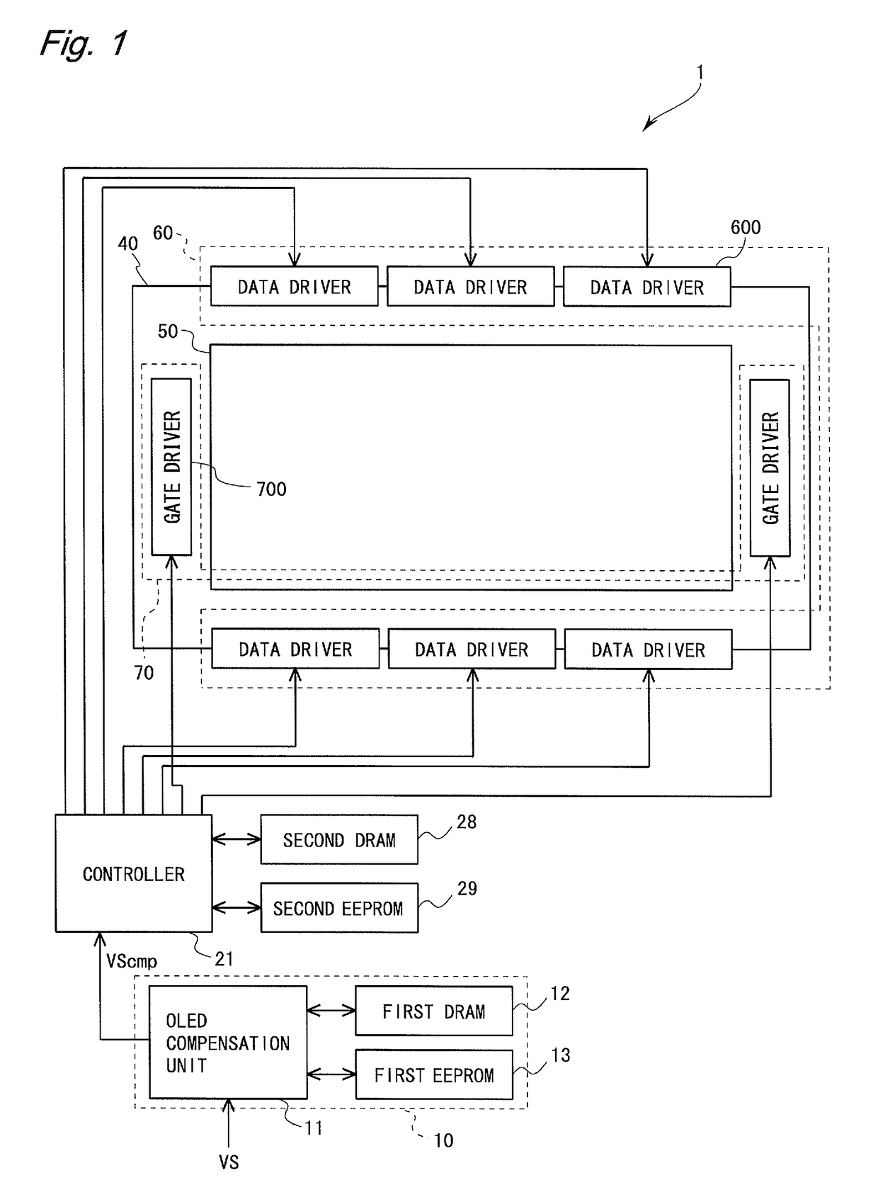
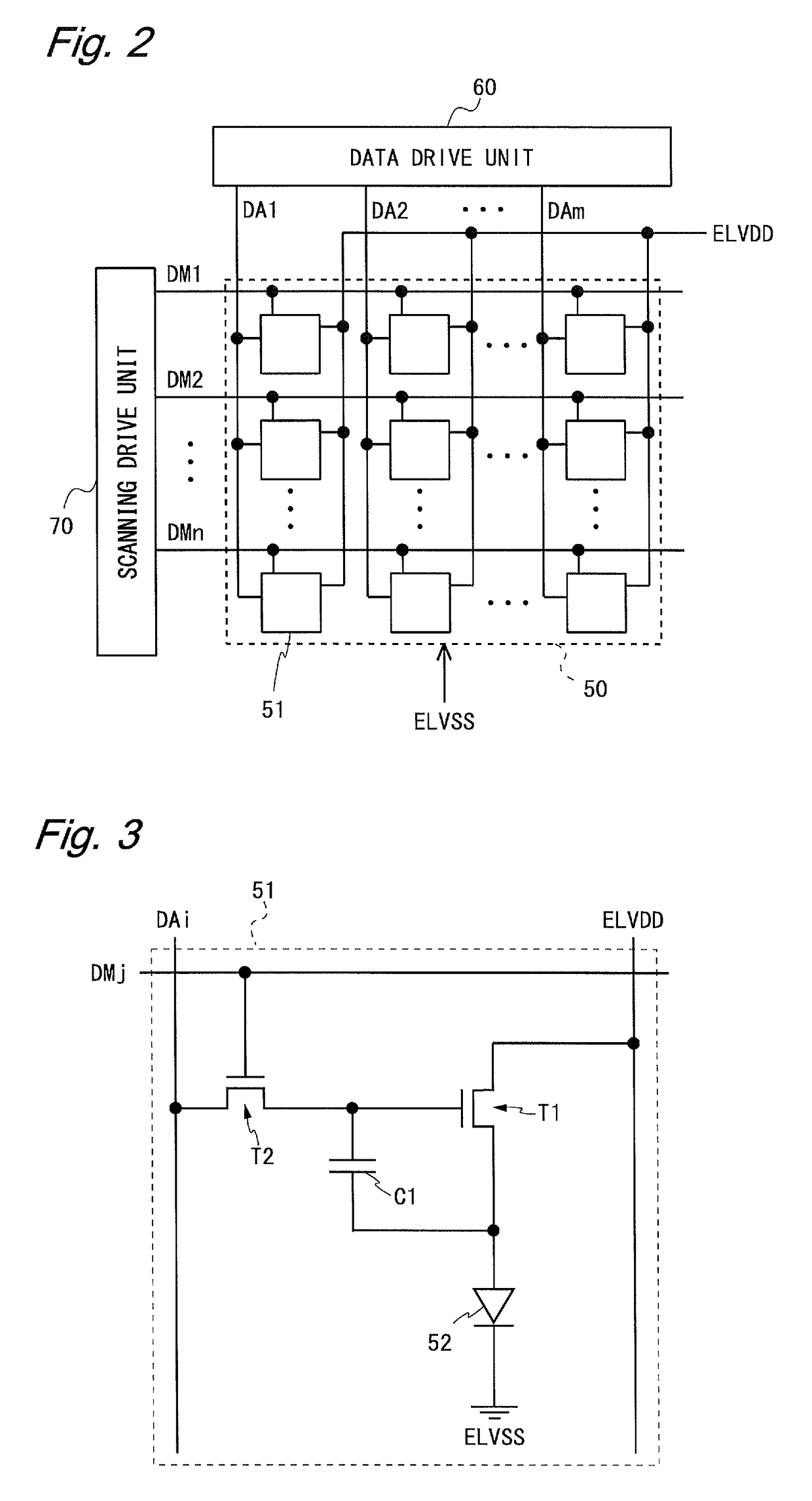
[0070]FIG. 1 is a block diagram showing a configuration of an active matrix-type organic EL display device 1 according to a first embodiment of the present invention. The organic EL display device 1 includes a data processing device 10, a controller 21 as a display control unit, a second dynamic random access memory (DRAM) 28, a second electrically erasable programmable read-only memory (EEPROM) 29, a display panel 40, a data drive unit 60, and a scanning drive unit 70. On the display panel 40, there are arranged the data drive unit 60 and the scanning drive unit 70. One or both of the data drive unit 60 and the scanning drive unit 70 may be integrally formed with the display unit 50. The second DRAM 28 and the second EEPROM may be provided inside the controller 21. The data processing device 10 includes an OLED compensation unit 11, a first DRAM 12, and a first EEPROM 13, and is realized as one chip set.
[0071]FIG. 2 is a block diagram for describing a confi...
second embodiment
2.1. Second Embodiment
[0121]
[0122]FIG. 10 is a block diagram showing a configuration of the active matrix-type organic EL display device 1 according to a second embodiment of the present invention. In the constituent elements of the present embodiment, for the elements same as those of the above first embodiment, the same reference characters are attached and the descriptions are omitted appropriately. The controller 21 in the present embodiment includes a TFT compensation unit 200. Each data driver 600 includes a data voltage supplying unit 610 and a current measurement unit 620. The data voltage supplying unit 610 has functions similar to those of the data driver 600 in the above first embodiment. The current measurement unit 620 measures a drive current obtained from the pixel circuit 51 in accordance with a data voltage based on drive gradation data, and acquires measurement data indicating a current value of the drive current. The current measurement unit 620 transmits the acqu...
third embodiment
3. Third Embodiment
[0179]
[0180]FIG. 15 is a block diagram showing a configuration of the active matrix-type organic EL display device 1 according to a third embodiment of the present invention. In the constituent elements of the present embodiment, for the elements same as those of the above first embodiment, the same reference characters are attached and the descriptions are omitted appropriately. In the present embodiment, the TFT compensation unit 200 is provided in the controller 21 in the above first embodiment. The configuration of the pixel circuit 51 may be similar to that in the above first embodiment or similar to that in the above second embodiment.
[0181]The TFT compensation unit 200 in the present embodiment performs various compensations without using the measurement data I, unlike that in the above second embodiment. As contents and techniques of compensation by the TFT compensation unit 200, all known contents and techniques can be employed, including the following, f...
PUM
 Abstract
Description
Claims
Application Information