Optical sensor device and a fingerprint sensor apparatus

Active Publication Date: 2017-12-14
NOVATEK MICROELECTRONICS CORP
View PDF5 Cites 15 Cited by
  • Summary
  • Abstract
  • Description
  • Claims
  • Application Information

AI Technical Summary

Benefits of technology

This patent describes an optical sensor device and a fingerprint sensor apparatus that are small in size and provide good sensing quality. The device includes a filter layer between the sensor layer and the microlens layer to reduce interference lights from the background. This results in a smaller device and improved sensing performance.

Problems solved by technology

Due to the optical lenses and the image sensing chip, the size of the optical device has some limitations.
For example, since the object distance and the image distance of the optical device have minimum values, the thickness of the optical fingerprint collection device is limited and difficult to be reduced.

Method used


Image

  • Optical sensor device and a fingerprint sensor apparatus
  • Optical sensor device and a fingerprint sensor apparatus
  • Optical sensor device and a fingerprint sensor apparatus

Examples


Embodiment Construction

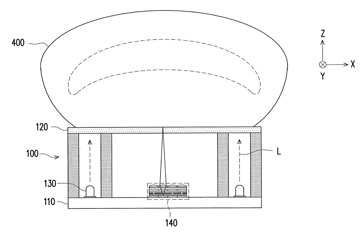
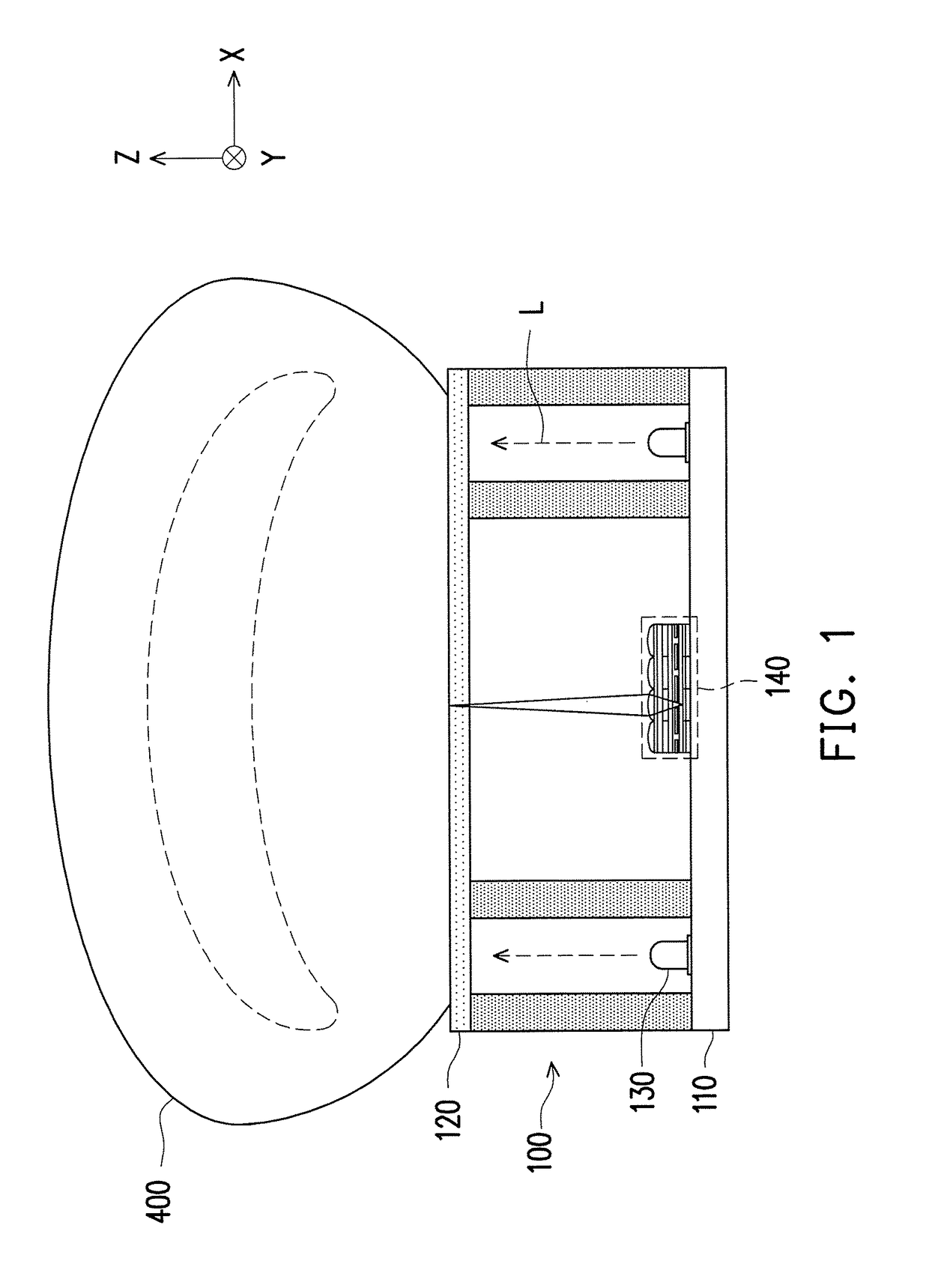
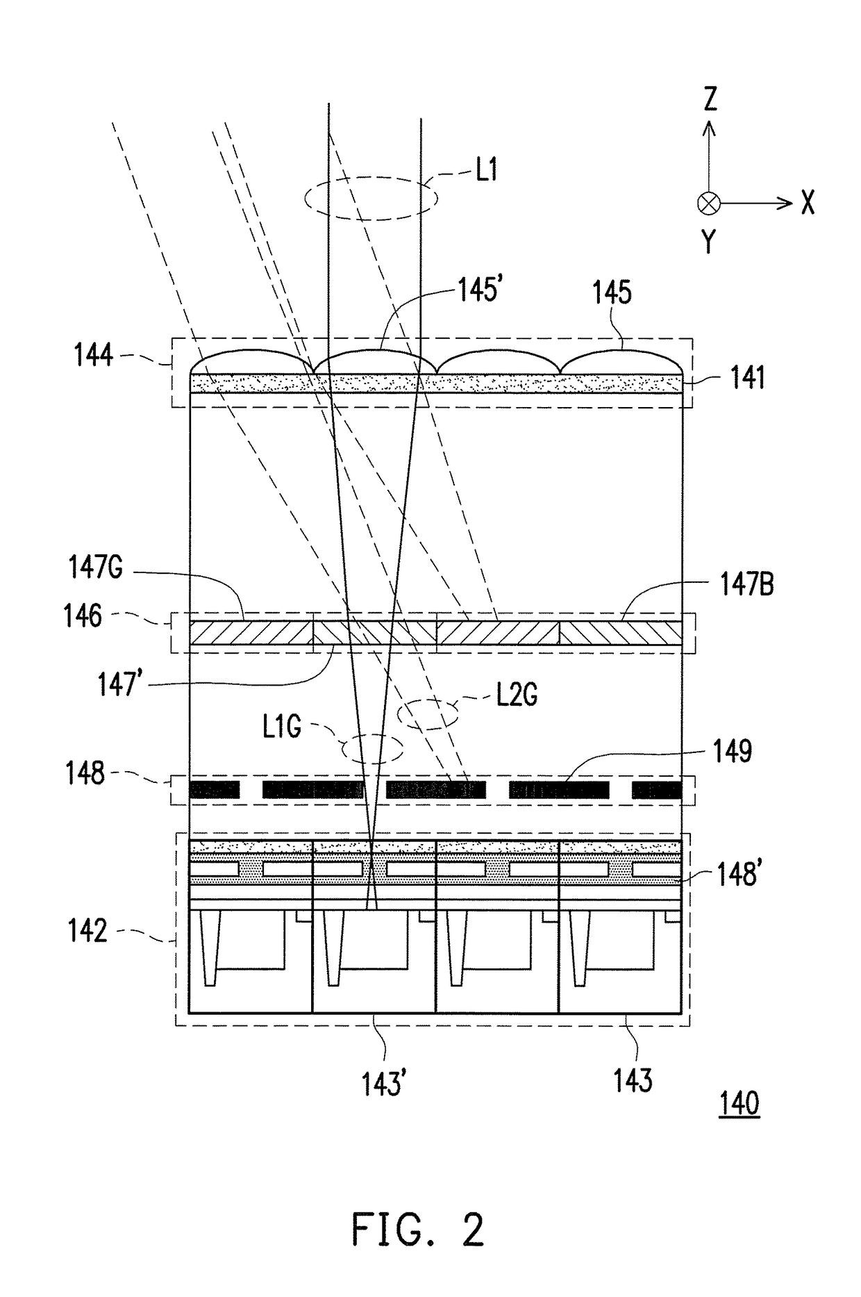
[0028]Reference will now be made in detail to the present preferred embodiments of the invention, examples of which are illustrated in the accompanying drawings. Wherever possible, the same reference numbers are used in the drawings and the description to refer to the same or like parts.

[0029]Embodiments are provided below to describe the disclosure in detail, though the disclosure is not limited to the provided embodiments, and the provided embodiments can be suitably combined. The term “coupling / coupled” and the phrase “electrically connecting / connected” used in this specification (including claims) of the application may refer to any direct or indirect connection means. For example, “a first device is coupled to a second device” should be interpreted as “the first device is directly connected to the second device” or “the first device is indirectly connected to the second device through other devices or connection means.” In addition, the term “signal” can refer to a current, a v...


PUM


Abstract

The optical sensor device including a sensor layer, a microlens layer and a filter layer is provided. The sensor layer includes a plurality of sensor areas, and is configured to sense a multi-wavelength light from a finger. The microlens layer includes a plurality of microlenses arranged in an array, and is disposed on the sensor layer. Each of the microlenses focuses the multi-wavelength light on a corresponding one of the sensor areas. The filter layer is disposed between the sensor layer and the microlens layer, and configured to filter the multi-wavelength light to generate a plurality of lights with different wavelengths. In addition, the fingerprint sensor apparatus including the foregoing optical sensor device is also provided.

Description

BACKGROUND OF THE INVENTION1. Field of the Invention[0001]The invention generally relates to an optical sensor device and a fingerprint sensor apparatus, in particular, to an optical sensor device and a fingerprint sensor apparatus capable of providing good sensing quality.2. Description of Related Art[0002]Optical devices such as optical fingerprint collection devices are widely used for fingerprint collection and identification. The collection of fingerprints through optical devices is based on optical imaging the finger surface through optical lenses. In addition, an image sensing chip is also required for the collection of fingerprints and built in the optical device. Due to the optical lenses and the image sensing chip, the size of the optical device has some limitations. For example, since the object distance and the image distance of the optical device have minimum values, the thickness of the optical fingerprint collection device is limited and difficult to be reduced.[0003]...

Claims


Application Information

Patent Timeline
IPC IPC(8): G06K9/00G02B5/20G02B3/00
CPCG06K9/00013G02B3/0056G02B5/201G06V40/1324G06V40/1318G06V10/147G06V40/13
Inventor CHEN, I-HSIUWANG, SHU-FANG
Owner NOVATEK MICROELECTRONICS CORP
Why Eureka
Try Eureka