Display device and manufacturing method thereof

Active Publication Date: 2021-06-24
SAMSUNG DISPLAY CO LTD
View PDF0 Cites 0 Cited by
  • Summary
  • Abstract
  • Description
  • Claims
  • Application Information

AI Technical Summary

Benefits of technology

The patent text describes a display device that can reduce the impact of electrical fields between a sensing electrode and a lower panel. This invention has a method for manufacturing this display device that can also reduce the impact of electrical fields.

Problems solved by technology

However, sensing electrodes and sensing lines may form conductive layers and parasitic capacitances in the display panel, thereby causing a deviation in touch sensitivity of the display device.

Method used


Image

  • Display device and manufacturing method thereof
  • Display device and manufacturing method thereof
  • Display device and manufacturing method thereof

Examples


Embodiment Construction

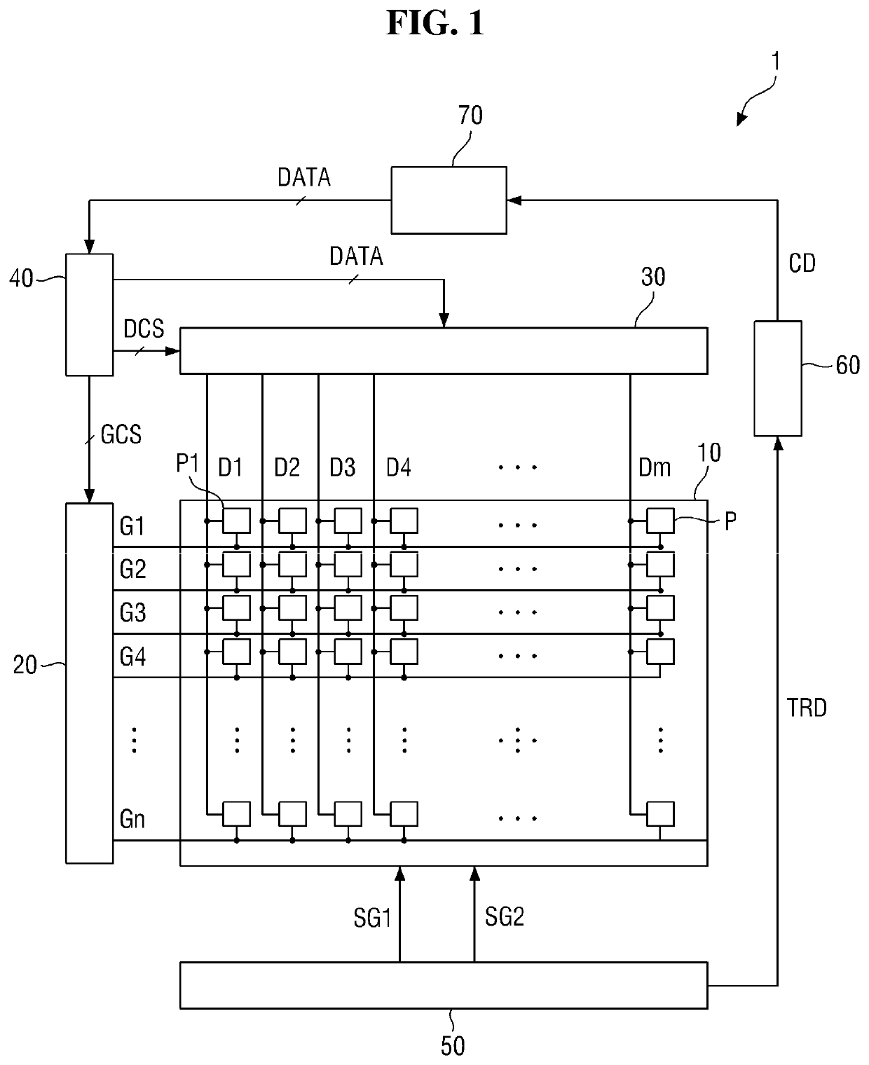
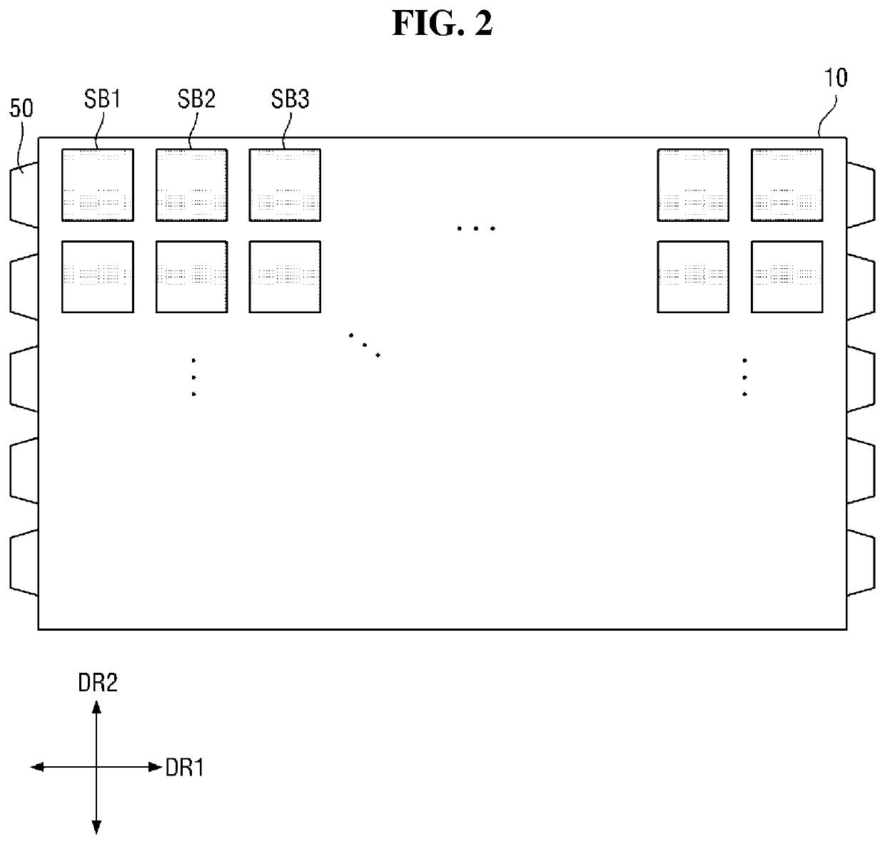
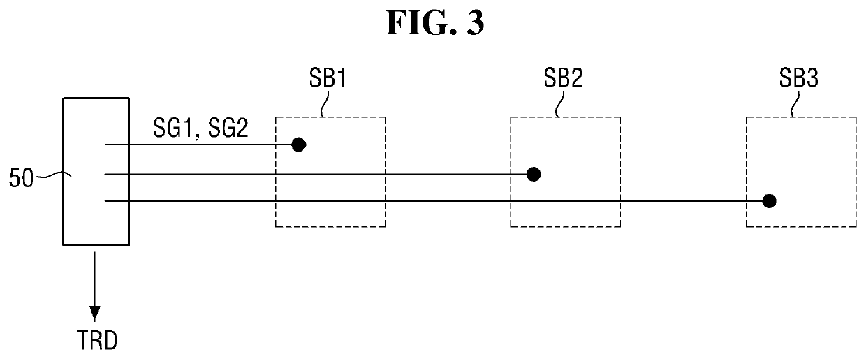
[0044]Specific structural and functional descriptions of embodiments disclosed herein are only for illustrative purposes of the embodiments of the invention. The embodiments may be embodied in many different forms without departing from the spirit and significant characteristics of the inventive concept. Therefore, the embodiments are disclosed only for illustrative purposes and should not be construed as limiting the inventive concept. That is, the inventive concept is only defined by the scope of the claims.

[0045]It will be understood that when an element is referred to as being related to another element such as being “coupled” or “connected” to another element, it can be directly coupled or connected to the other element or intervening elements may be present therebetween. In contrast, it should be understood that when an element is referred to as being related to another element such as being “directly coupled” or “directly connected” to another element, there are no intervenin...


PUM


Abstract

A display device includes a lower panel including a first substrate and at least one transistor disposed on the first substrate; and an upper panel facing the lower panel and including a first touch conductive layer including a second substrate, sensing electrodes disposed on the second substrate and including a first sensing electrode, and sensing lines including a second sensing line, a first insulating layer disposed on the first touch conductive layer, and a second touch conductive layer disposed on the first insulating layer including a blocking layer overlapping the sensing electrodes and the sensing lines and a connection electrode overlapping the first sensing electrode, the first sensing line, and the second sensing line.

Description

[0001]This application claims priority under 35 U.S.C. § 119 to Korean Patent Application No. 10-2019-0171714 filed on Dec. 20, 2019 in the Korean Intellectual Property Office, the disclosure of which is incorporated by reference herein in its entirety.BACKGROUND1. Field[0002]The present disclosure relates to a display device and a manufacturing method of the display device.2. Description of the Related Art[0003]The importance of a display device has increased with the development of multimedia. Accordingly, various types of display devices such as a liquid crystal display (LCD) and an organic light emitting display (OLED) have been used.[0004]Among display devices, a liquid crystal display device, which is one of the most widely used flat panel display devices, includes two substrates including electric field generating electrodes such as a pixel electrode and a common electrode and a liquid crystal layer disposed in between the pixel electrode and the common electrode. In the liqu...

Claims


Application Information

Patent Timeline
IPC IPC(8): G02F1/1333G06F3/041G06F3/044G02F1/1335
CPCG02F1/13338G06F3/0412G02F1/133512G06F3/0446G06F3/0445G06F3/0443G02F1/136286G02F1/1343G06F3/041G06F2203/04103
Inventor SEO, YUN MINKIM, TAE GYUNPARK, YONG DOOLEE, BUM
Owner SAMSUNG DISPLAY CO LTD
Why Eureka
Try Eureka