Passive amplification circuit and analog-digital convertor

Active Publication Date: 2014-07-24
RENESAS ELECTRONICS CORP
View PDF4 Cites 21 Cited by
  • Summary
  • Abstract
  • Description
  • Claims
  • Application Information

AI Technical Summary

Benefits of technology

[0028]According to the embodiment, it becomes possible to avoid a high-speed charging and discharging operation because the reference of the common-mode voltage is not used for the passive amplifier. Also, with

Problems solved by technology

Also, an error efficient of an analog circuit which is a cause to degrade the effective resolution of the analog-digital converter, contains a non-linear error, a DC offset

Method used


Image

  • Passive amplification circuit and analog-digital convertor
  • Passive amplification circuit and analog-digital convertor
  • Passive amplification circuit and analog-digital convertor

Examples


Example

Conventional Example 1

[0069]In Non-Patent Literature 1, a method of simply realizing signal amplification by using a capacitance has been described. In this method, capacitances connected in parallel are stacked in serial upon sampling a signal so as to obtain a voltage with the magnitude of about twice.

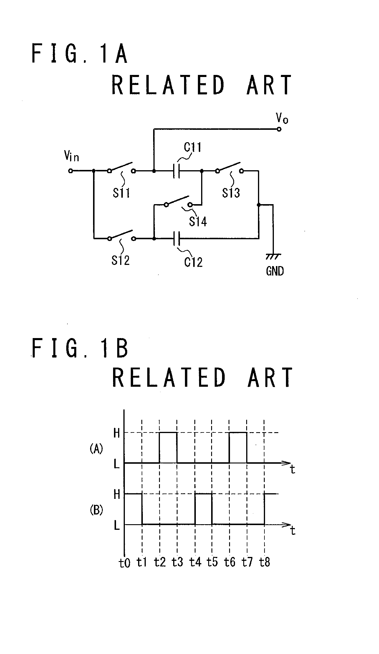
[0070]FIG. 1A is a diagram schematically showing a configuration example of the passive amplification circuit according to the conventional example 1.

[0071]The components of the passive amplification circuit shown in FIG. 1A will be described. The passive amplification circuit shown in FIG. 1A has a first capacitance C11, a second capacitance C12, an input terminal Vin, an output terminal Vo, the ground voltage GND, and a first switch S11 to a fourth switch S14. Here, the first capacitance C1 and the second capacitance C2 have a same capacitive amount or capacitance.

[0072]The connection relation of the respective components shown in FIG. 1A will be described. The input terminal Vin i...

Example

Conventional Example 2

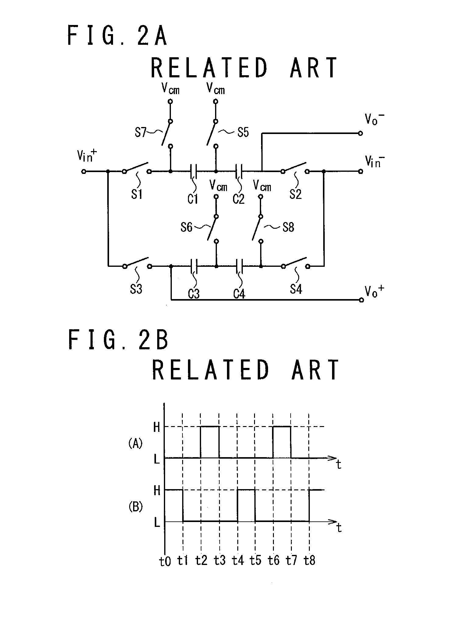
[0084]FIG. 2A is a diagram schematically showing a configuration example of the passive amplification circuit according to the conventional example 2.

[0085]The components of the passive amplification circuit shown in FIG. 2A will be described. The passive amplification circuit shown in FIG. 2A has the first capacitance C1 to the fourth capacitance C4, the positive side input terminal of Vin+, the negative side input terminal Vin−, the positive side output terminal Vo+, the negative side output terminal Vo−, a reference voltage supply end Vcm, a first switch S1 to an eighth switch S8. Here, the first capacitance C1 to the fourth capacitance C4 have a same capacitance. The positive side input terminal Vin+ and the negative side input terminal Vin− respectively input a positive side voltage and a negative side voltage of an input signal. The positive side output terminal Vo+ and the negative side output terminal Vo− respectively output a positive side voltage and ...

Example

Conventional Example 3

[0093]FIG. 3A is a diagram schematically showing a configuration example of the passive amplification circuit according to the conventional example 3.

[0094]The component of the passive amplification circuit shown in FIG. 3A will be described. The passive amplification circuit shown in FIG. 3A has the first capacitance C1, the second capacitance C2, the positive side input terminal Vin+, the negative side input terminal Vin−, the positive side output terminal Vo+, the negative side output terminal Vo−, the reference voltage supply end Vcm, the first switch S1 to the sixth switch S6. Here, the first capacitance C1 and the second capacitance C2 have completely the same capacitance. The positive side input terminal Vin+ and the negative side input terminal Vin− input the positive side voltage and the negative side voltage of the input signal, respectively. The positive side output terminal Vo+ and the negative side output terminal output the positive side voltage a...


PUM


Abstract

A differential signal is amplified by passive amplification which does not a reference of a common-mode voltage. At this time, the voltage of the differential signal is passive-amplified twice before carrying out a successive approximation type analog-digital conversion operation. The passive amplification is attained by providing a plurality of capacitances which carry out a sampling operation, and switching these connection relation by using switches. Without being accompanied by the increase of the consumed power and the chip size, an influence by the noise of s comparator is reduced to a half so that the effective resolution can be increased for one bit.

Description

CROSS REFERENCE[0001]This application claims priorities on convention based on Japanese Patent Application Nos. JP 2013-010218 and JP 2013-259954. The disclosure thereof is incorporated herein by reference.TECHNICAL FIELD[0002]The present invention is related to a passive amplification circuit and an analog-digital convertor, and more particularly, to a passive amplification circuit having the voltage gain of 1 to 2 times, and an analog-digital convertor suitable for a charge share type successive approximation type analog-digital convertor.BACKGROUND ART[0003]Conventionally, a configuration is generally used in which correct signal amplification is carried out by using a closed amplifier for a circuit which contains an amplification stage thereinside, such as a pipeline ADC (Analog-Digital Converter).[0004]However, although the closed amplifier can realize amplification in a high precision, it causes the increase of the consumed power in a high-speed operation. As a result, it is t...

Claims


Application Information

Patent Timeline
IPC IPC(8): H03M1/12H03F1/32
CPCH03F1/3211H03M1/124G11C27/02H03M1/44H03F3/45475H03H7/004H03F3/45071H03F2203/45171H03F2203/45544H03M1/002H03M1/38H03F1/02H03F3/005H03M1/1009
Inventor OKUDA, YUICHINAKANE, HIDEOYAMAMOTO, TAKAYAKIMURA, KEISUKEOSHIMA, TAKASHIMATSUURA, TATSUJI
Owner RENESAS ELECTRONICS CORP
Why Eureka
Try Eureka