Semiconductor device

Active Publication Date: 2007-05-31
RENESAS ELECTRONICS CORP
View PDF13 Cites 20 Cited by
  • Summary
  • Abstract
  • Description
  • Claims
  • Application Information

AI Technical Summary

Benefits of technology

[0018] For the solution of the above-described problem, the inventor has noticed the importance of a sense circuit capable of determining the data in the memory cell even with a slight shift in bit-line potential. Furthermore, the inventor has devised a circuit capable of not only performing the determination with a slight shift in bit-line potent

Problems solved by technology

Therefore, a decrease in potent

Method used


Image

  • Semiconductor device
  • Semiconductor device
  • Semiconductor device

Examples


Example

[0036] Hereinafter, embodiments of the present invention will be described in detail with reference to the accompanying drawings. Note that components having the same function are denoted by the same reference symbols throughout the drawings for describing the embodiment, and the repetitive description thereof will be omitted.

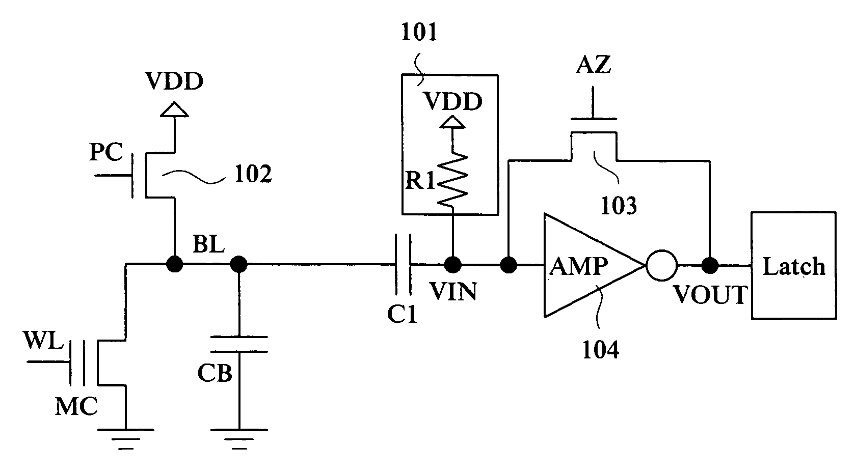
[0037]FIG. 1 is a circuit diagram showing the configuration of a read sense circuit in a non-volatile semiconductor storage device according to one embodiment of the present invention.

[0038] First, an example of the configuration of the non-volatile semiconductor storage device according to this embodiment will be described with reference to FIG. 1. The non-volatile semiconductor storage device according to this embodiment is, for example, a flash memory, and it includes a non-volatile memory cell MC, a bit line BL connected to the memory cell MC, a capacitor C1 (first capacitor) with one end connected to the bit line BL, an inverter 104 (inverting amplifier ...


PUM


Abstract

A semiconductor storage device in which a read sense circuit stable for the fluctuation in manufacturing process and environmental conditions can be realized and the read access time can be shortened is provided. A sense circuit for reading a memory cell characterized in that a flowing current is varied depending on stored data and a voltage applied through a word line includes: an inverter; a first capacitor provided so as to be electrically connected between an input of the inverter and a bit line to which the memory cell is connected; a first transistor which short-circuits an input and an output of the inverter; a second capacitor for supplying charge to the first capacitor; and second transistors, wherein an input potential of the inverter is increased or decreased according to the current of the memory cell and is then amplified to be latched as a logic value.

Description

CROSS-REFERENCE TO RELATED APPLICATION [0001] The present application claims priority from Japanese Patent Application No. JP 2005-335861 filed on Nov. 21, 2005, the content of which is hereby incorporated by reference into this application. TECHNICAL FIELD OF THE INVENTION [0002] The present invention relates to a non-volatile semiconductor storage device. More particularly, it relates to a technology effectively applied to a non-volatile semiconductor storage device using, as a memory cell, a current-type memory cell such as a floating-gate-type flash memory, a discrete-trap MONOS, a SONOS-type memory, a phase change memory, or an MRAM (magnetic random access memory), in which a resistance of the memory cell and a current flowing through the memory cell are changed depending on stored data. BACKGROUND OF THE INVENTION [0003] According to the study by the inventor of the present invention, for example, the following technology is known in a non-volatile semiconductor storage device...

Claims


Application Information

Patent Timeline
IPC IPC(8): G11C7/10
CPCG11C7/065G11C7/067G11C7/12G11C11/5642G11C11/5678G11C13/0004G11C13/0026G11C13/004G11C16/26H01L27/115H10B69/00
Inventor KAJIYAMA, SHINYA
Owner RENESAS ELECTRONICS CORP
Why Eureka
Try Eureka