Design enhanced 3D printed support block

a technology of 3d printing and support blocks, which is applied in the field of 3d printing support blocks, can solve the problems of flat support not working, components on the bottom side of the circuit board could be damaged, and the top of the board could be uneven, so as to achieve uniform application of solder paste, improve dimensional tolerance, and reduce weight

Active Publication Date: 2022-03-10
JABIL INC
View PDF0 Cites 0 Cited by
  • Summary
  • Abstract
  • Description
  • Claims
  • Application Information

AI Technical Summary

Benefits of technology

[0018]The disclosed exemplary apparatuses, systems, and methods provide a 3D printed support that can be utilized in a screen-printing process to achieve a more uniform application of solder paste on a printed circuit board or printed circuit boa...

Problems solved by technology

However, for circuit boards with components on both sides, a flat support does not work because of the presence of the components.
The components on the bottom side of the circuit board could be damaged from being compressed between a flat support and the circuit board.
Additionally, a top of the board would likely be uneven when components are present on the bottom of the board and the support is flat.
While the aforementioned support blocks have been useful in screen printing processes, they do not provide optimal surface flatness.
This problem is compounded by the two-block design because there is a dimensional tolerance (variation) for each block and the total dime...

Method used


Image

  • Design enhanced 3D printed support block
  • Design enhanced 3D printed support block
  • Design enhanced 3D printed support block

Examples


Embodiment Construction

[0039]The following detailed description and appended drawings describe and illustrate various embodiments of the invention. The description and drawings serve to enable one skilled in the art to make and use the invention, and are not intended to limit the scope of the invention in any manner. In respect of the methods disclosed, the steps presented are exemplary in nature, and thus, the order of the steps is not necessary or critical

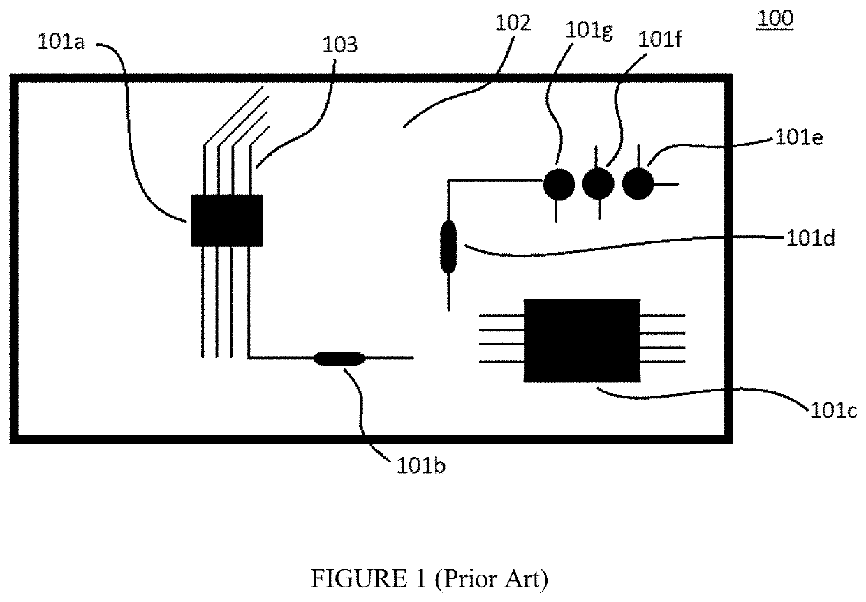
[0040]FIG. 1 shows a printed circuit board assembly (PCBA) 100. The PCBA 100 contains components, represented in FIG. 1 as 101a, b, c, d, e, f, and g, that are attached to a printed circuit board (PCB) 102. Traces 103 are used to carry electrons from one location to another. The components 101a, b, c, d, e, f, and g are three dimensional and extend from the PCB.

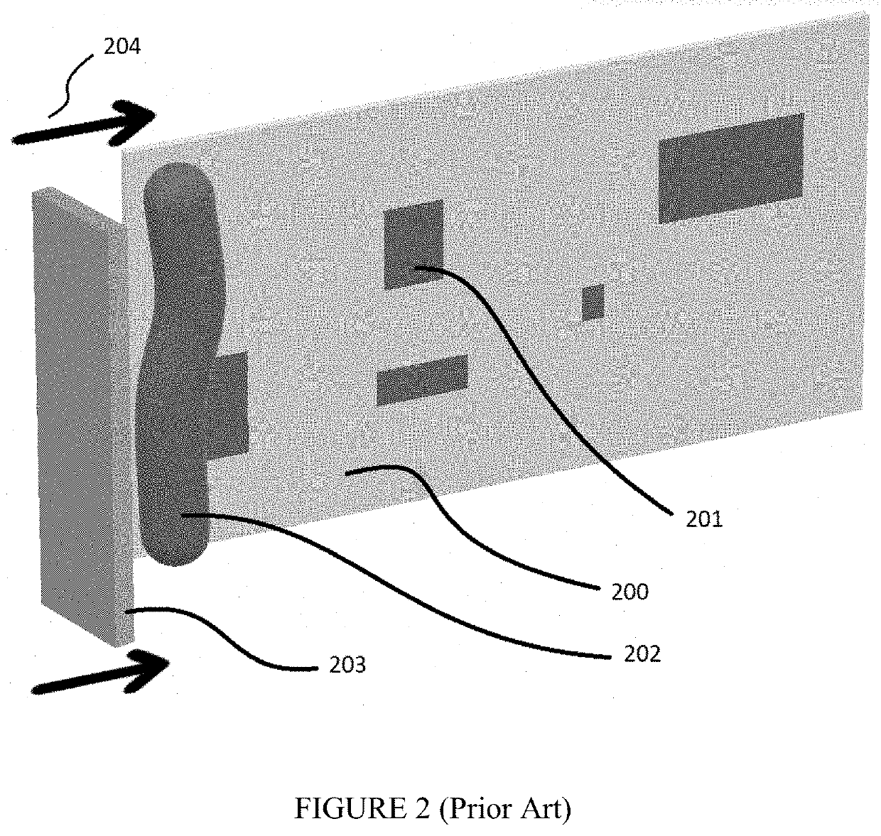
[0041]FIG. 2 shows an apparatus that is commonly used to screen print solder paste onto the PCB 102. A stencil 200 contains apertures 201 (and other apertures as shown by squares and rectangles ...


PUM

PropertyMeasurementUnit
Thermoplasticityaaaaaaaaaa
Attractive forceaaaaaaaaaa

Abstract

Support blocks for printed circuit boards (PCB's) and printed circuit board assemblies (PCBA's), wherein the support blocks are produced from a 3D printing process. The support block including a bottom surface having a vacuum connection; a top surface having at least one vacuum hole; at least one recessed surface that is offset from the top surface; and at least one vacuum channel extending from the vacuum connection to the at least one vacuum hole.

Description

FIELD[0001]The present disclosure relates to the field of 3D printed support blocks for screen printed circuit board assemblies, test fixtures, go-no-go fixtures, wave soldering pallets, and the like.BACKGROUND[0002]This section provides background information related to the present disclosure which is not necessarily prior art. A printed circuit board assembly (PCBA), comprises a printed circuit board (PCB) that contains electrically conductive traces to carry electrons from one location to another. These traces are typically made of copper and allow electrons to flow from one component to another. Components include integrated circuits, resistors, capacitors, diodes, and others. Surface mount technology (SMT) describes a method whereby electrical components are mounted directly onto a surface of a printed circuit board.[0003]In the SMT process, screen printers can be used to deposit solder paste at defined locations on a PCB. Solder paste contains small amounts of conductive metal...

Claims


Application Information

Patent Timeline
IPC IPC(8): H05K13/00B25B11/00B29C64/364
CPCH05K13/0069B25B11/005B33Y10/00B25B11/002B29C64/364B33Y80/00H05K2203/0173H05K3/3485H05K3/00H05K2203/0165B41F15/08B41F15/18B41F15/34B41F15/46
Inventor BURGESS, DARINCROCKETT, RANDYDEROSETT, TIMOTHYSANTHAKUMAR, CHARLESKLIMCZAK, SCOTTMOHAMMED, ANWAR A.RODGERS, LUKESINGH, HARPUNEETTORRES, DANIELTORRES, FELIPE
Owner JABIL INC
Why Eureka
Try Eureka