Method for multi-band communication and electronic device thereof

a multi-band communication and electronic device technology, applied in the direction of wireless communication, transmission, electrical apparatus, etc., can solve the problems of increasing the cost of electronic devices, increasing the complexity of electronic devices, so as to increase the data rate through multi-band communication, low complexity and cost

Pending Publication Date: 2022-05-05
SAMSUNG ELECTRONICS CO LTD
View PDF29 Cites 0 Cited by
  • Summary
  • Abstract
  • Description
  • Claims
  • Application Information

AI Technical Summary

Benefits of technology

[0010]According to various example embodiments disclosed in the present disclosure, an electronic device may increase the data rate through multi-band communication.
[0011]According to various example ...

Problems solved by technology

The electronic device using such an MMTC may have relatively low functionality and cost.
In order to support multi-band communication, th...

Method used


Image

  • Method for multi-band communication and electronic device thereof
  • Method for multi-band communication and electronic device thereof
  • Method for multi-band communication and electronic device thereof

Examples


Embodiment Construction

[0024]Hereinafter, various example embodiments of the disclosure will be described with reference to the accompanying drawings. However, this is not intended to limit the present disclosure to the specific embodiments, and it is to be construed to include various modifications, equivalents, and / or alternatives of embodiments of the present disclosure.

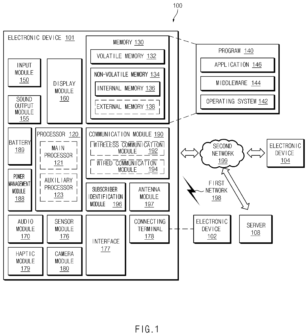
[0025]FIG. 1 is a block diagram illustrating an example electronic device 101 in a network environment 100 according to various embodiments. Referring to FIG. 1, the electronic device 101 in the network environment 100 may communicate with an electronic device 102 via a first network 198 (e.g., a short-range wireless communication network), or at least one of an electronic device 104 or a server 108 via a second network 199 (e.g., a long-range wireless communication network). According to an embodiment, the electronic device 101 may communicate with the electronic device 104 via the server 108. According to an embodiment, the electronic...


PUM


Abstract

Disclosed is an electronic device including: first communication circuitry including a first amplifier, second communication circuitry including a second amplifier, a transceiver, a processor, and a power supply. The processor may be configured to: provide, to the first communication circuitry, a first voltage for transmitting a first signal using the power supply in a first time interval, and provide, to the second communication circuitry, a second voltage for transmitting a second signal using the power supply in a second time interval that does not overlap the first time interval.

Description

CROSS-REFERENCE TO RELATED APPLICATIONS[0001]This application is a continuation of International Application No. PCT / KR2021 / 015280 designating the United States, filed on Oct. 28, 2021, in the Korean Intellectual Property Receiving Office and claiming priority to Korean Patent Application No. 10-2020-0144230 filed on Nov. 2, 2020, in the Korean Intellectual Property Office, the disclosures of which are incorporated by reference herein in their entireties.BACKGROUNDField[0002]The disclosure relates to a method for multi-band communication and an electronic device thereof.Description of Related Art[0003]In order to improve data throughput, communication using multiple bands is widely used. For example, an electronic device may perform carrier aggregation using a plurality of frequency bands. The electronic device may perform carrier aggregation using a primary component carrier (PCC) and a secondary component carrier (SCC) associated with a base station. For example, the electronic de...

Claims


Application Information

Patent Timeline
IPC IPC(8): H04B1/401H04B1/52H04W72/04
CPCH04B1/401H04W72/0473H04B1/52
Inventor MOON, YOHANNA, HYOSEOK
Owner SAMSUNG ELECTRONICS CO LTD
Why Eureka
Try Eureka