Three-dimensional semiconductor memory device and method of fabricating the same

a semiconductor memory and three-dimensional technology, applied in semiconductor devices, semiconductor/solid-state device details, electrical devices, etc., can solve the problem of limited practicality of increasing integration for two-dimensional, and achieve the effect of increasing integration density

Active Publication Date: 2022-07-14
SAMSUNG ELECTRONICS CO LTD
View PDF7 Cites 0 Cited by
  • Summary
  • Abstract
  • Description
  • Claims
  • Application Information

AI Technical Summary

Benefits of technology

This approach enables higher integration density and cost-effective manufacturing of three-dimensional semiconductor memory devices, overcoming the limitations of two-dimensional devices by allowing for more efficient use of semiconductor substrate space and reducing the need for expensive equipment.

Problems solved by technology

However, expensive process equipment needed to increase pattern fineness sets a practical limitation on increasing integration for two-dimensional or planar semiconductor devices.

Method used


Image

  • Three-dimensional semiconductor memory device and method of fabricating the same
  • Three-dimensional semiconductor memory device and method of fabricating the same
  • Three-dimensional semiconductor memory device and method of fabricating the same

Examples


Embodiment Construction

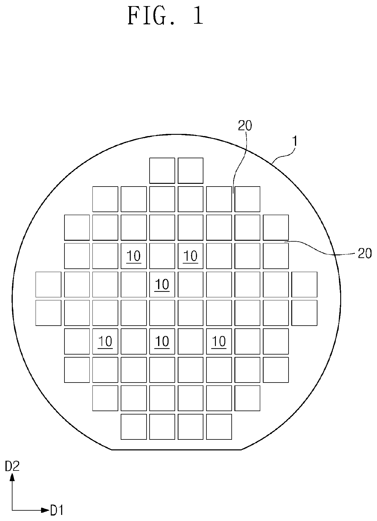
[0029]A three-dimensional semiconductor memory device according to an embodiment of the inventive concept and a method of fabricating the same will be described in more detail below with reference to the accompanying drawings.

[0030]FIG. 1 is a diagram illustrating a substrate, on which three-dimensional semiconductor memory devices are integrated according to an embodiment of the inventive concept.

[0031]Referring to FIG. 1, a semiconductor substrate 1 (e.g., a wafer) may include chip regions 10, from which semiconductor chips are respectively formed, and a scribe line regions, respective ones which are located between the chip regions 10. The chip regions 10 may be two-dimensionally arranged in two different directions (e.g., the first direction D1 and a second direction D2 shown in FIG. 1). Each of the chip regions 10 may be surrounded by scribe line regions 20. A corresponding scribe line region 20 may be disposed between each adjacent pair of the chip regions 10, which are adjace...


PUM


Abstract

A three-dimensional semiconductor memory device may include horizontal patterns disposed on a peripheral circuit structure and spaced apart from each other, memory structures provided on the horizontal patterns, respectively, each of the memory structures including a three-dimensional arrangement of memory cells. Penetrating insulating patterns and separation structures may isolate the horizontal patterns from one another. Through vias may extend through the penetrating insulating patterns to connect logic circuits of the peripheral circuit structure to the memory structure.

Description

CROSS-REFERENCE TO RELATED APPLICATIONS[0001]This U.S. non-provisional patent application is a divisional of U.S. application Ser. No. 16 / 777,776 filed Jan. 30, 2020, which claims priority under 35 U.S.C. § 119 to Korean Patent Application No. 10-2019-0075814, filed on Jun. 25, 2019, in the Korean Intellectual Property Office, the entire contents of each of which are hereby incorporated by reference.BACKGROUND OF THE INVENTION[0002]The present disclosure relates to a three-dimensional semiconductor memory device and a method of fabricating the same, and in particular, to a highly-integrated three-dimensional semiconductor memory device and a method of fabricating the same.[0003]Higher integration of semiconductor devices is required to satisfy consumer demands for superior performance and inexpensive prices. In the case of semiconductor devices, since their integration is an important factor in determining product prices, increased integration is especially required. Integration of ...

Claims


Application Information

Patent Timeline
Patent Type & AuthorityApplications(United States)
IPC IPC(8): H01L27/11582H01L27/11526H01L27/11556H01L23/522H01L23/528H01L21/28H01L29/66H01L27/11519H01L27/11565H01L27/11573H10B41/00H10B43/27H10B41/10H10B41/20H10B41/27H10B41/30H10B41/35H10B41/40H10B43/10H10B43/35H10B43/40
CPCH01L27/11582H01L27/11526H01L27/11556H01L23/5226H01L23/528H01L29/40114H01L29/66545H01L27/11519H01L27/11565H01L27/11573H01L29/40117H10B41/00H10B41/20H10B41/35H10B41/30H10B41/10H10B41/50H10B43/10H10B43/50H10B41/27H10B43/27H01L29/792H10B43/40H10B43/35H10B41/40
InventorYANG, WOOSUNGLEE, DONG-SIKHWANG, SUNG-MINLIM, JOON-SUNG
OwnerSAMSUNG ELECTRONICS CO LTD