Check patentability & draft patents in minutes with Patsnap Eureka AI!

Semiconductor integrated circuit for radio communication

a technology of integrated circuits and radio communication, applied in the direction of radio transmission, transmission, substation equipment, etc., can solve the problems of wasteful current consumption wasteful current consumption, etc., and achieve the effect of improving the rising characteristics of a power source and reducing current consumption

Active Publication Date: 2007-03-06
PANNOVA SEMIC
View PDF9 Cites 5 Cited by
  • Summary
  • Abstract
  • Description
  • Claims
  • Application Information

AI Technical Summary

Benefits of technology

[0007]It is an object of the present invention to provide a semiconductor integrated circuit for radio communication having a power source control system capable of operating / stopping element circuits not only together as a single functional block but also separately as individual circuits, thereby making it possible to reduce current consumption and improve the rising characteristics of a power source.

Problems solved by technology

Among individual circuits contained in a functional block, power is supplied to a circuit(s) not in use when the corresponding functional block is operated, so that current is wastefully consumed.
However, when power source control is performed on the each functional block basis, it is required to operate a whole block for processing a receiving voice band signal, resulting in wasteful current consumption.
Furthermore, when a semiconductor integrated circuit for radio communication having a voice signal level detector is used, even in a radio communication apparatus that does not use a voice signal level detector, it is required to operate a whole block for processing a transmission voice band signal, resulting in wasteful current consumption.
Also, there is a problem with a noise detector that is used in combination with an intermediate frequency detector for the purpose of detecting the level of a receiving signal.
However, when power source control is performed on the each functional block basis, it is required to operate a whole block for processing a receiving high frequency signal, resulting in wasteful current consumption.
On the other hand, when power source control is performed on the each functional block basis only for the purpose of reducing current consumption, load fluctuation associated with the operation / stop of an element circuit has an influence on another element circuit connected thereto in the same functional block, resulting in deterioration of the rising characteristics of a power source.

Method used


Image

  • Semiconductor integrated circuit for radio communication
  • Semiconductor integrated circuit for radio communication
  • Semiconductor integrated circuit for radio communication

Examples


embodiment 1

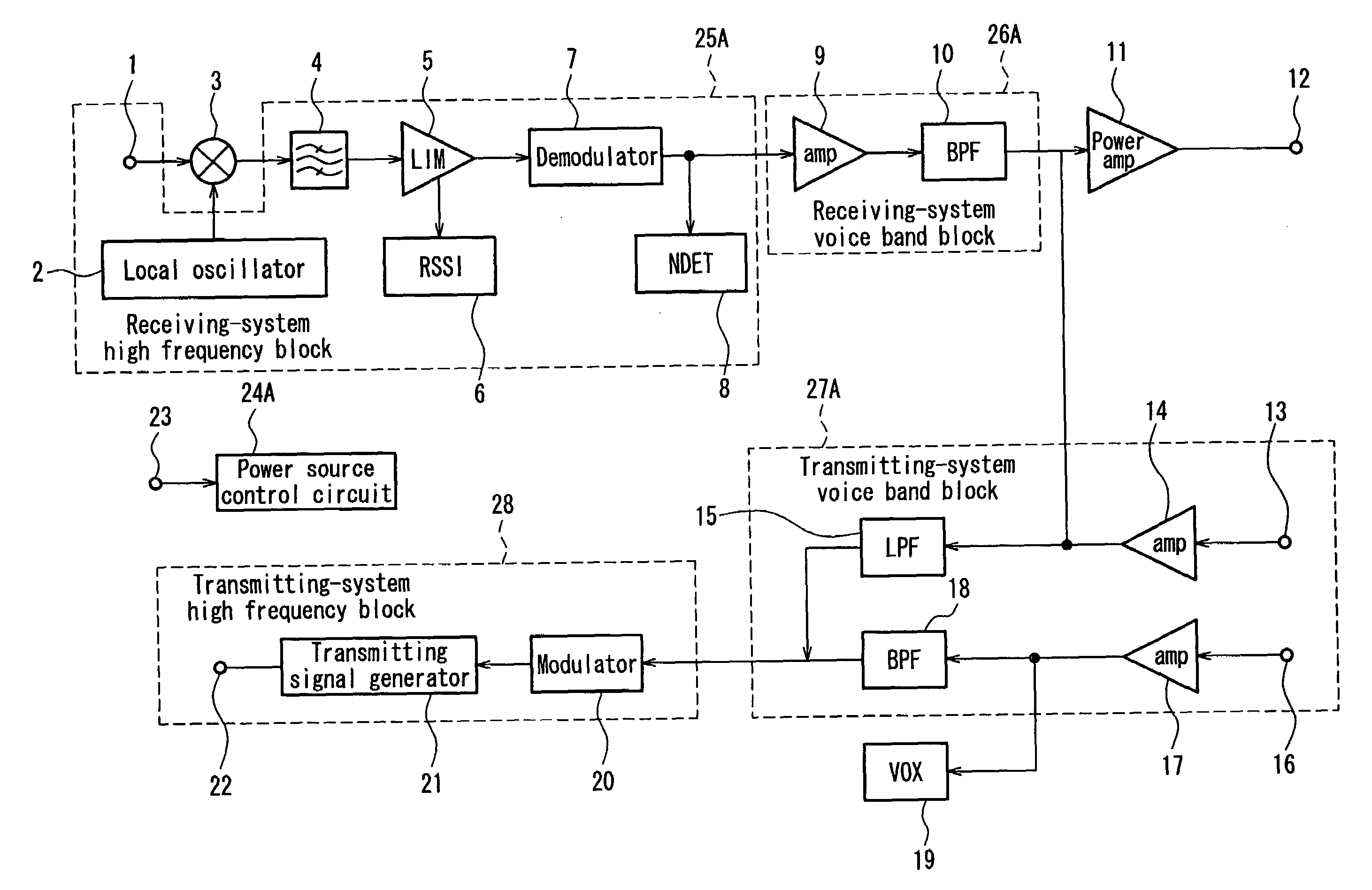
[0036]FIG. 2 is a block diagram showing a semiconductor integrated circuit for radio communication according to Embodiment 1 of the present invention. In FIG. 2, the same element circuits as those of FIG. 1 are referenced with the same reference numerals and the explaination is not repeated. The semiconductor integrated circuit for radio communication of Embodiment 1 is different from that of FIG. 1 in that element circuits included in a receiving-system high frequency block 25A, a receiving-system voice band block 26A, and a transmitting-system voice band block 27A are changed, and accordingly, power source control is performed by a power source control circuit 24A. Table 1 shows the groups to be controlled based on this power source control system.

[0037]

TABLE 1Groups toElement circuitsbe controlledincluded in a block25AReceiving-system high2Local signal generatorfrequency block4Intermediate frequency signalbandpass filter5Intermediate frequencyamplifier6Intermediate frequency dete...

embodiment 2

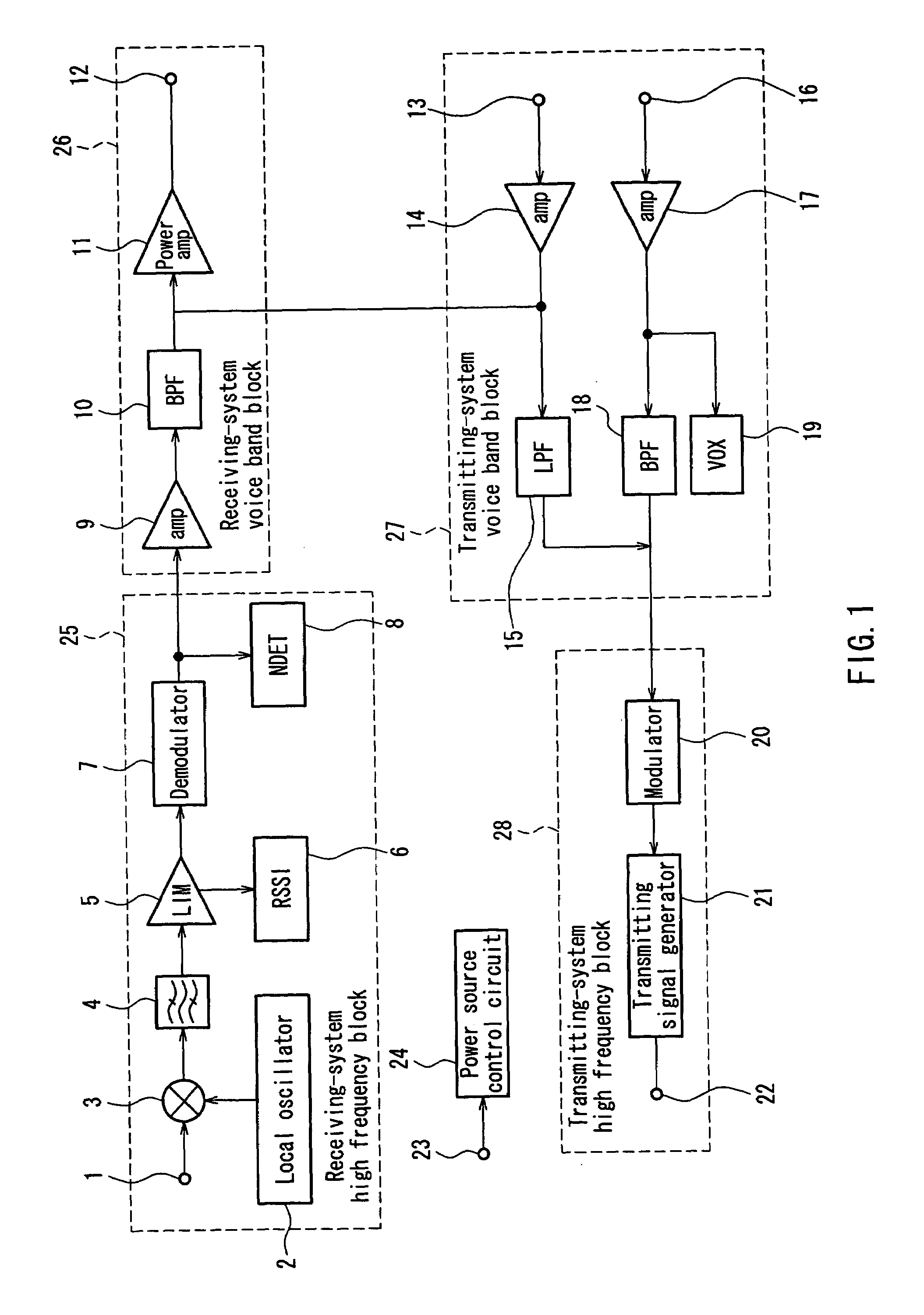
[0043]FIG. 3 is a block diagram showing a semiconductor integrated circuit for radio communication according to Embodiment 2 of the present invention. In FIG. 3, the same element circuits as those of FIG. 1 are referenced with the same reference numerals and the explanation is not repeated. The semiconductor integrated circuit for radio communication of Embodiment 2 is different from that of FIG. 1 in that element circuits in a receiving-system voice band block 26A are changed, and accordingly, power source control is performed by a power source control circuit 24B. Table 2 shows the groups to be controlled based on this power source control system.

[0044]

TABLE 2Groups to beElement circuitscontrolledincluded in a block25Receiving-system high2Local signal generatorfrequency block3Multiplicator4Intermediate frequency signalbandpass filter5Intermediate frequencyamplifier6Intermediate frequency detector7Demodulator8Noise detector26AReceiving-system9Received voice signal amplifiervoice ba...

embodiment 3

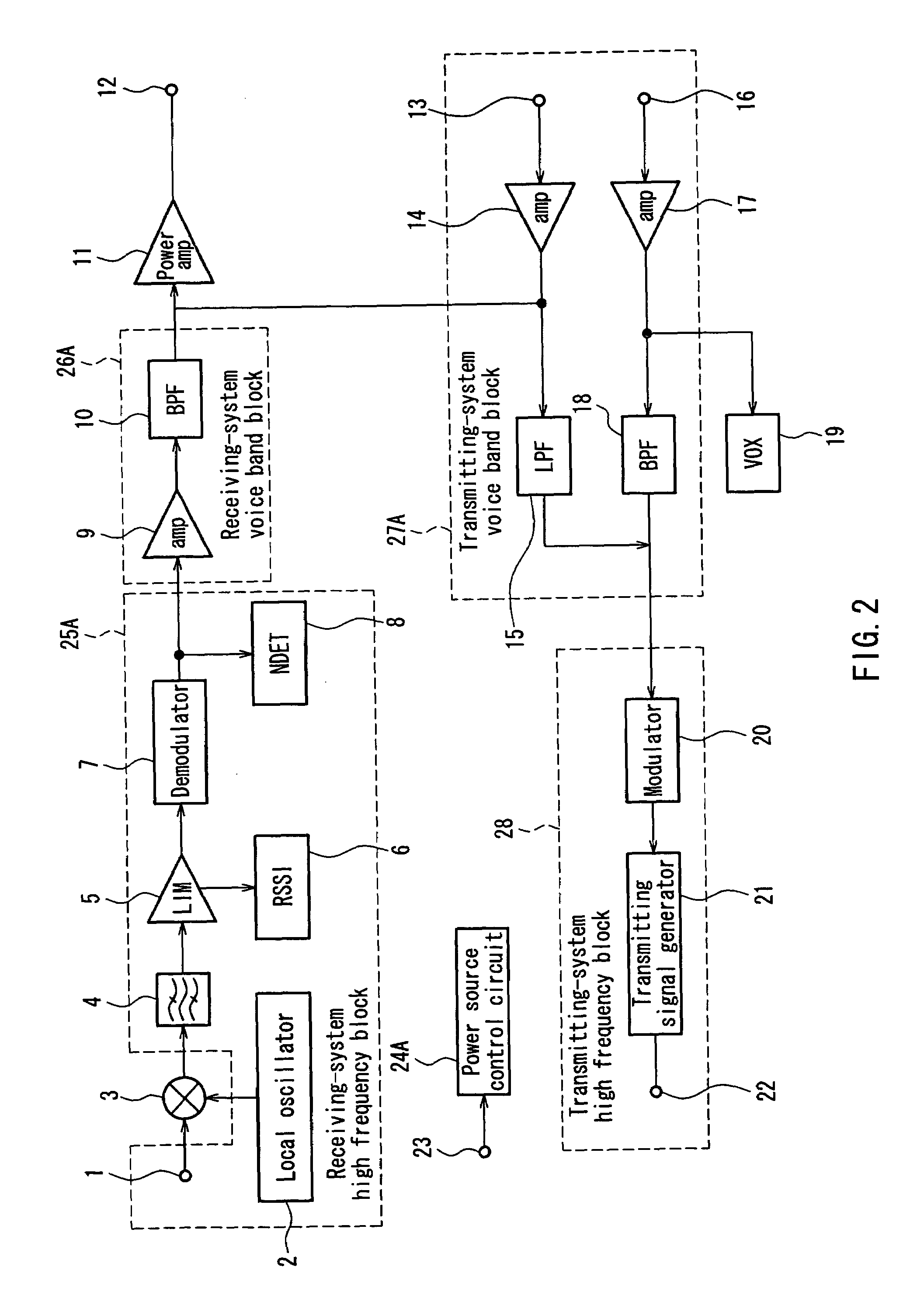
[0048]FIG. 4 is a block diagram showing a semiconductor integrated circuit for radio communication according to Embodiment 3 of the present invention. In FIG. 4, the same element circuits as those of FIG. 1 are referenced with the same reference numerals and the explanation is not repeated. The semiconductor integrated circuit for radio communication of Embodiment 3 is different from that of FIG. 1 in that element circuits in a transmitting-system voice band block 27A are changed, and accordingly, power source control is performed by a power source control circuit 24C. Table 3 shows the groups to be controlled based on this power source control system.

[0049]

TABLE 3Groups to beElement circuitscontrolledincluded in a block25Receiving-system high2Local signal generatorfrequency block3Multiplicator4Intermediate frequency signalbandpass filter5Intermediate frequencyamplifier6Intermediate frequency detector7Demodulator8Noise detector26Receiving-system voice9Received voice signal amplifier...


PUM


Abstract

A semiconductor integrated circuit for radio communication includes a receiving-system high frequency block, a receiving-system voice band block, a transmitting-system voice band block, a transmitting-system high frequency block, and a power source control circuit for performing power source control to operate / stop each of the groups of circuits based on a power source control signal. The power source control circuit performs individual power source control for at least one circuit of the multiplier, the noise detector, the voice signal power amplifier, and the voice signal level detector, and also performs the power source control for each of the receiving-system high frequency block, the receiving-system voice band block, the transmitting-system voice band block, and the transmitting-system high frequency block, except for the at least one circuit subjected to the individual power source control.

Description

FIELD OF THE INVENTION[0001]The present invention relates to a semiconductor integrated circuit for radio communication. More particularly, the present invention relates to a semiconductor integrated circuit for radio communication that uses a power source control system capable of operating / stopping a plurality of circuits together as a single functional block or separately as individual circuits.BACKGROUND OF THE INVENTION[0002]When a semiconductor integrated circuit for radio communication is used in an apparatus for mobile communication, power consumption needs to be minimized for prolonged battery life. To achieve this, power source control is performed so that the operation of a circuit involved in a function that is not currently used during the call waiting state or the like, is stopped. For example, JP H06-232349A describes power source control that is performed to operate / stop each functional block, but not individual circuits separately. In other words, a different power ...

Claims


Application Information

Patent Timeline
Patent Type & Authority Patents(United States)
IPC IPC(8): H04B1/38H01Q11/12H04B1/04H04B1/06H04B1/40H04B1/44H04B7/00
CPCH04B1/44H04B1/40
Inventor YAMAGUCHI, SATOSHI
Owner PANNOVA SEMIC
Features
  • R&D
  • Intellectual Property
  • Life Sciences
  • Materials
  • Tech Scout
  • Unparalleled Data Quality
  • Higher Quality Content
  • 60% Fewer Hallucinations
Learn More