Electromagnetic wave absorptive film and its fabrication

a technology of electromagnetic waves and absorption films, applied in the field of electromagnetic protective materials, can solve the problems of limiting the application range, dna destructive diseases, and high risk of leukaemia, and achieve the effects of eliminating the installation of grounding, effective absorption of electromagnetic waves, and thin thickness

Inactive Publication Date: 2007-07-10
YEN LI HSIEN
View PDF2 Cites 3 Cited by
  • Summary
  • Abstract
  • Description
  • Claims
  • Application Information

AI Technical Summary

Benefits of technology

[0009]It is another object of the present invention to provide an electromagnetic wave absorptive film and its fabrication method, which has a thin thickness practical for use in any of a variety of products to effectively absorb electromagnetic waves.
[0010]It is still another object of the present invention to provide an electromagnetic wave absorptive film and its fabrication method, which eliminates the installation of grounding without causing electric connection.

Problems solved by technology

In consequence, consumers have a high chance of exposing the body to the harm of electromagnetic waves that may result in a high risk of leukaemia, encephalophyma, DNA destructive disease, and other diseases.
According to studies, electromagnetic waves over 60 Hz become harmful to DNA in human cells.
However, conventional EMI protective materials commonly have a certain thickness that limits the application range.
When conventional EMI protective materials are used in small mobile electronic products, electromagnetic waves will still leak.

Method used


Image

  • Electromagnetic wave absorptive film and its fabrication
  • Electromagnetic wave absorptive film and its fabrication
  • Electromagnetic wave absorptive film and its fabrication

Examples


Embodiment Construction

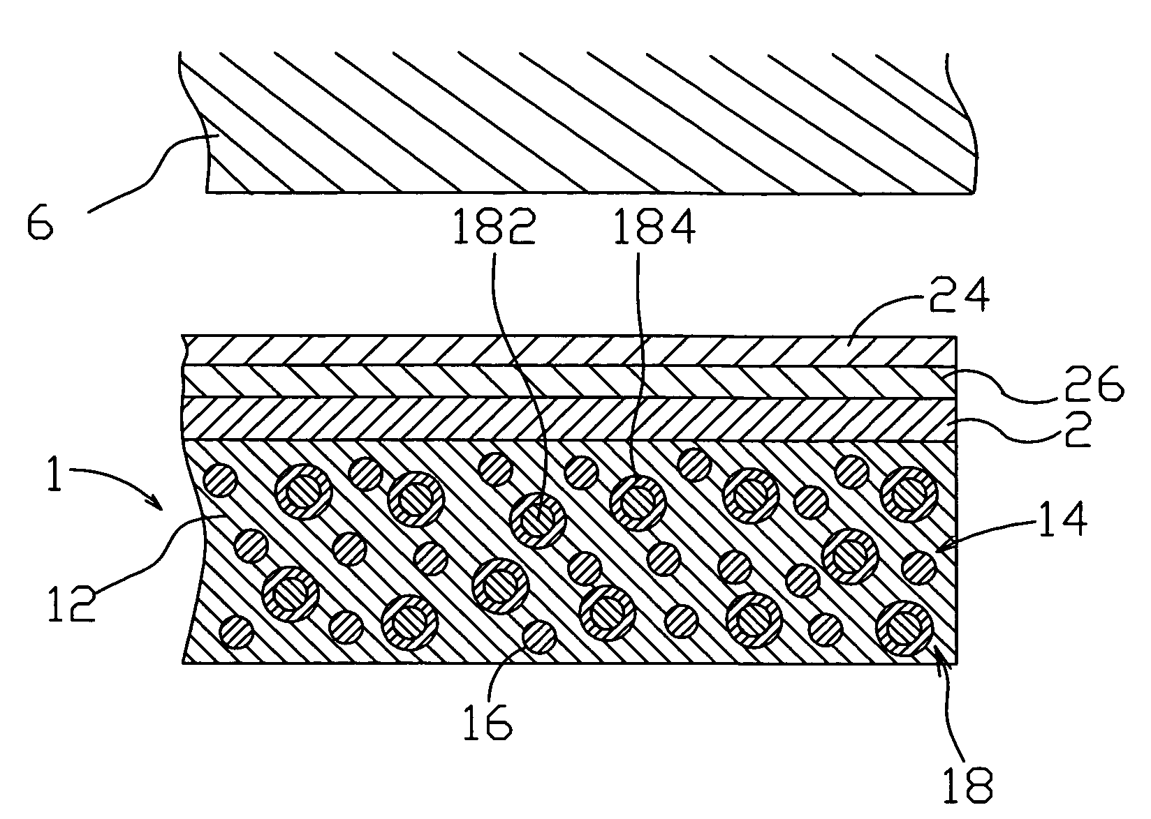
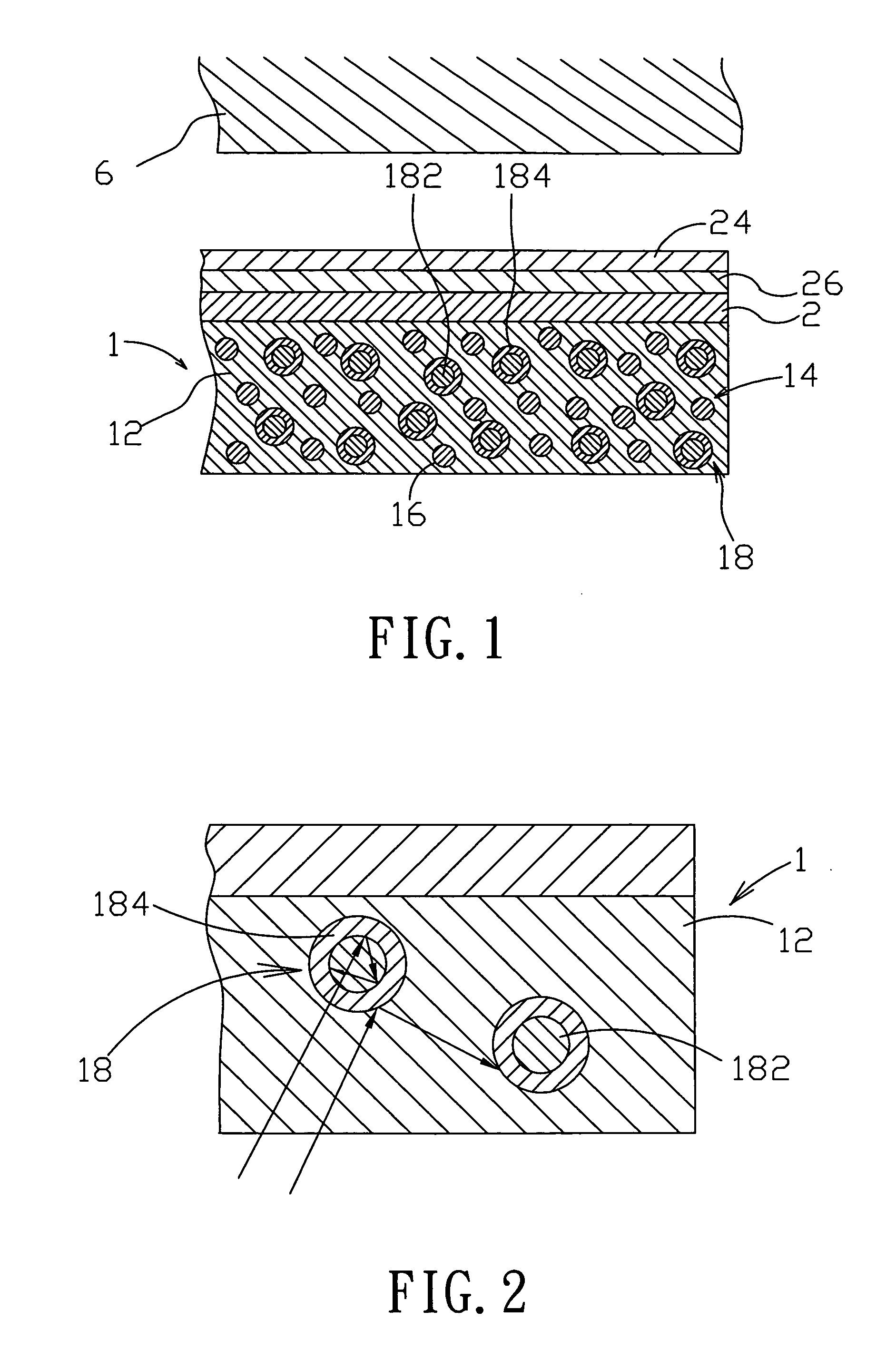
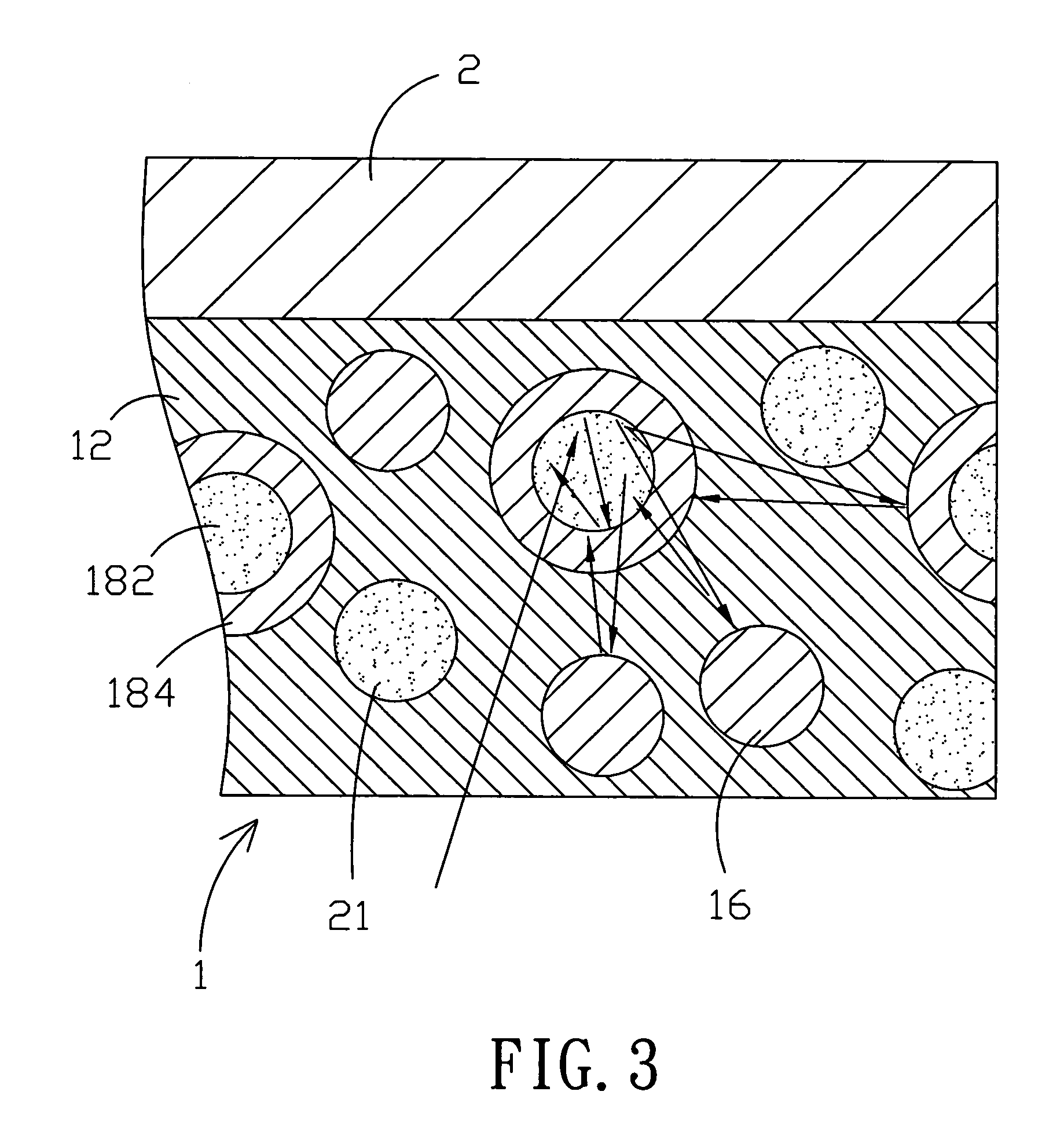
[0019]An electromagnetic wave absorptive film in accordance with the present invention utilizes destructive interference to absorb electromagnetic waves. The so-called destructive interference is to have two reversed wave trains of same wavelength meet each other, enabling the peaks of one wave train to be respectively overlapped on the wave troughs of another wave train, and therefore the two wave trains are neutralized.

[0020]FIG. 1 is a schematic drawing showing the relationship between an electromagnetic wave absorptive film and a product 6 to be shield. As illustrated, the electromagnetic wave absorptive film comprises a compound layer 1 and a reflective layer 2 covered on one side, namely, the top side of the compound layer 1. The compound layer 1 is comprised of a carrier 12, and grains 14 embedded in the carrier 12. The carrier 12 is prepared from a polymeric material. The thickness of the compound layer 1 meets the requirement for destructive interference, i.e., ¼n times of ...


PUM

PropertyMeasurementUnit
electromagnetic wave absorptiveaaaaaaaaaa
thicknessaaaaaaaaaa
refractive indexaaaaaaaaaa

Abstract

An electromagnetic wave absorptive film for absorbing electromagnetic waves by means of destructive interference is disclosed to include a compound layer, which has single-layer and / or double-layer wave-absorbing and / or wave reflecting grains embedded therein and a thickness equal to ¼n times of the wavelength of the electromagnetic wave to be absorbed, and a reflective layer, which is covered on one side of the compound layer and has a refractive index greater than the compound layer.

Description

BACKGROUND OF THE INVENTION[0001]1. Field of the Invention[0002]The present invention relates to EMI protective materials and more particularly, to an electromagnetic wave absorptive film that absorbs electromagnetic waves by means of destructive interference. The invention relates also to the fabrication of such an electromagnetic wave absorptive film.[0003]2. Description of the Related Art[0004]Following fast development of high technology, a variety of computers and digitalized communication apparatus and consumer electronic products have been disclosed and have appeared on the market. It is the market trend to make electronic products of relatively higher frequency. In consequence, consumers have a high chance of exposing the body to the harm of electromagnetic waves that may result in a high risk of leukaemia, encephalophyma, DNA destructive disease, and other diseases. According to studies, electromagnetic waves over 60 Hz become harmful to DNA in human cells. Some other forei...

Claims


Application Information

Patent Timeline
Patent Type & Authority Patents(United States)
IPC IPC(8): G02F1/03
CPCB32B33/00H05K9/0088B32B37/12B32B2307/206
Inventor YEN, LI-HSIEN
Owner YEN LI HSIEN
Why Eureka
Try Eureka