Substrate for and a process in connection with the product of structures

a technology of substrate and product, applied in the direction of individual molecule manipulation, fluid speed measurement, optical light guide, etc., can solve the problems of uneven structure on the substrate, structural variations in the surface material of the flat plate, uneven surface embedding,

Inactive Publication Date: 2004-01-08
OBDUCAT AB SE
View PDF8 Cites 76 Cited by
  • Summary
  • Abstract
  • Description
  • Claims
  • Application Information

AI Technical Summary

Problems solved by technology

One problem in connection with the NIL process is that there are structural variations in the material in the surface of a flat plate, or in other words there is, on a nanometre scale, an irregularity in the surface of each plate (template and substrate) even if the plates are polished.
These irregularities result in an undesirable uneven distribution of force over the surfaces when the template and substrate are pressed together, which in turn leads to an unevenly embedded structure on the substrate.
One problem that is not mentioned in this regard, however, is that it is not possible to achieve intervals (periods) between the structural parts that are of as small a size as the structural parts themselves using the method described.
However, such profiles are impossible to create directly when the template is pressed down into the coating layer of the substrate.
If the NIL process is to be a

Method used


Image

  • Substrate for and a process in connection with the product of structures
  • Substrate for and a process in connection with the product of structures
  • Substrate for and a process in connection with the product of structures

Examples


first embodiment

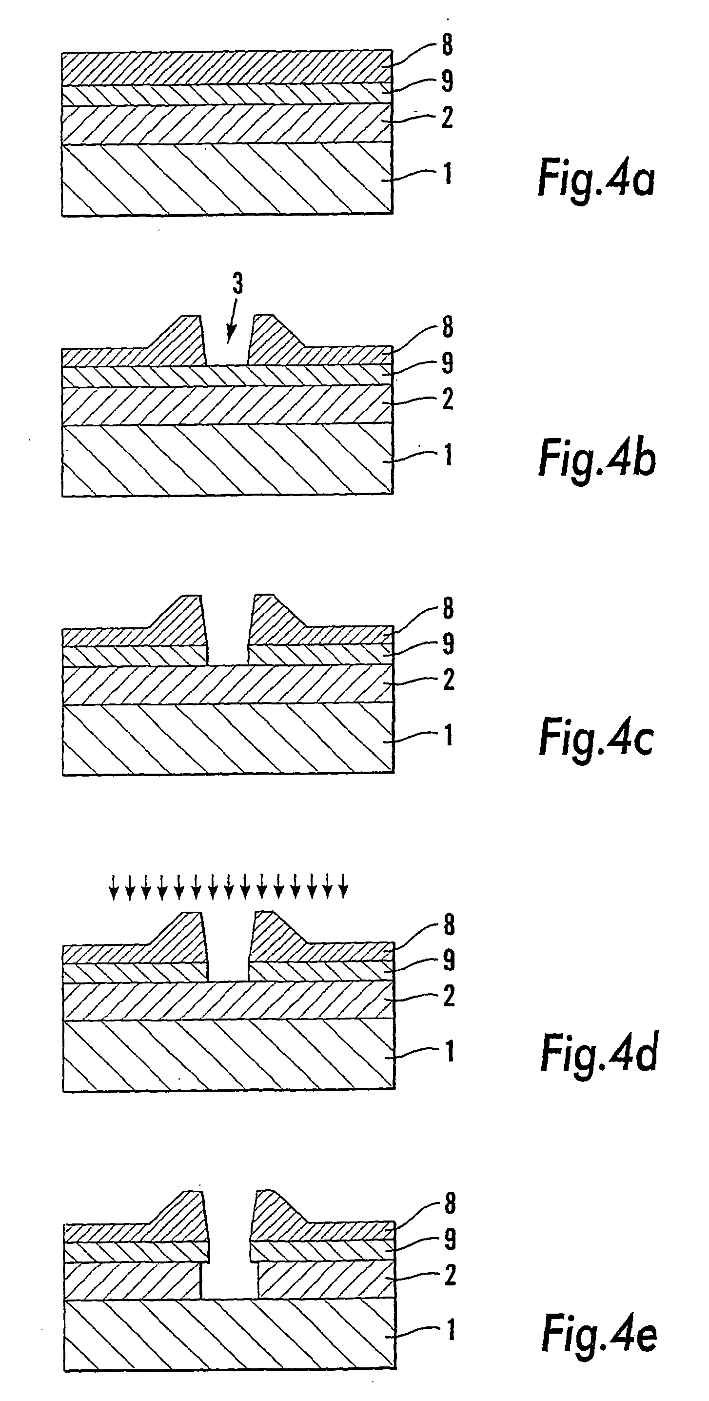
[0033] FIGS. 4a-e show a coated substrate according to the invention and the stages for NIL of the same,

second embodiment

[0034] FIGS. 5a-c show a coated substrate according to the invention and the stages for NIL of the same,

third embodiment

[0035] FIGS. 6a-d show a coated substrate according to the invention and the stages for NIL of the same,

[0036] FIG. 7 shows a preferred device, seen from the side in cross-section, for execution of the imprint stage,

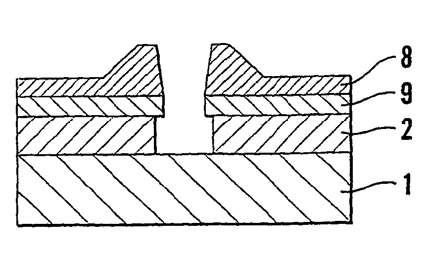
[0037] FIG. 8a shows a scanning electron microscope image of a coated, nanoimprinted and developed substrate according to the invention,

[0038] FIG. 8b shows a sketch of the substrate in FIG. 8a with reference to different parts in the same,

[0039] FIGS. 9a-b show scanning electron microscope images of a substrate according to the prior art, following "lift-off", a single layer of resist having been used,

[0040] FIGS. 9c-d show scanning electron microscope images of a substrate according to the invention following "lift-off".

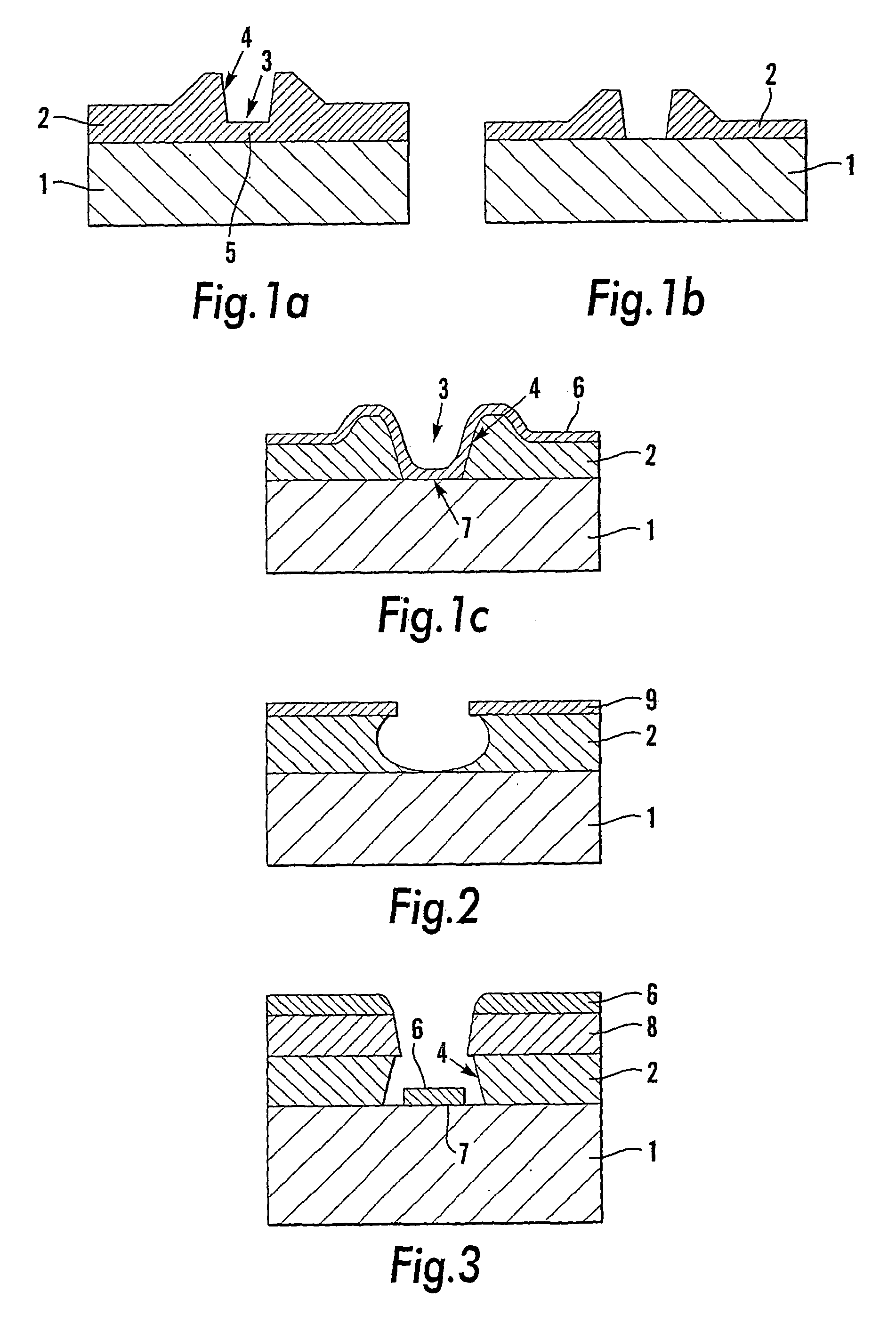
[0041] According to the above problem description, it is important for an undercut profile to be produced in the coating layer / layers on the substrate. FIG. 1a shows a substrate that has been coated with a coating layer 2 (a resist) according to the pri...


PUM

PropertyMeasurementUnit
Thicknessaaaaaaaaaa
Angleaaaaaaaaaa
Nanoscale particle sizeaaaaaaaaaa

Abstract

The invention relates to a substrate (1) comprising at least a first (2) and a second (8) coating layer on one surface of the substrate, for nanoimprint lithography, said first coating layer (2) consisting of a positive resist and said second (8) coating layer consisting of a negative resist. The invention also relates to a process in connection with nanoimprint lithography on the substrate (1), a pattern (3) of nanometre size being impressed in a first stage into the second coating layer (8) by means of a template (610), following which the first coating layer (2), in a second stage, is exposed to a chiefly isotropic developing method on surfaces thereof that have been exposed in connection with said first stage, a method for developing and material for said first and second coating layers being selected so that the first coating layer (2) is developed more quickly than the second coating layer (8), so that an undercut profile is obtained in the coating layers.

Description

[0001] The present invention relates to a substrate including at least a first and a second coating layer on one surface of the substrate, for nanoimprint lithography.[0002] The invention also relates to a process in connection with the lithography of structures of nanometre size on a coated substrate. The invention is applicable in connection with nanoimprint lithography on semiconductor materials, such as silicon, indium phosphide or gallium arsenide, for the production of semiconductor components, but also in connection with nanoimprint lithography on other rigid materials, such as ceramic materials, metals or polymers with a relatively high glass transition temperature, for use in e.g. biosensors.PRIOR ART[0003] The trend in microelectronics is towards ever smaller dimensions. In principle, development has been such that the dimensions are halving every third year. Commercial components are being manufactured today with structures of roughly 200 nm in size, but there is a need t...

Claims


Application Information

Patent Timeline
IPC IPC(8): G03F7/004B81B1/00B82B1/00G03F7/095G03F7/20G03F7/26H01L21/027H01L21/033
CPCG03F7/095Y10T428/24942H01L21/0331
Inventor HEIDARI, BABAK
Owner OBDUCAT AB SE
Why Eureka
Try Eureka