
Substrate-guided optical device utilizing thin transparent layer
a technology of optical devices and transparent layers, applied in the field of substrate-guided optical devices, can solve the problems of inconvenient installation, unsafe use, and state-of-the-art huds, and achieve the effects of convenient integration, large eye-motion-box values, and convenient design and fabrication
- Summary
- Abstract
- Description
- Claims
- Application Information
AI Technical Summary
Benefits of technology
Problems solved by technology
Method used
Image

Examples
Embodiment Construction
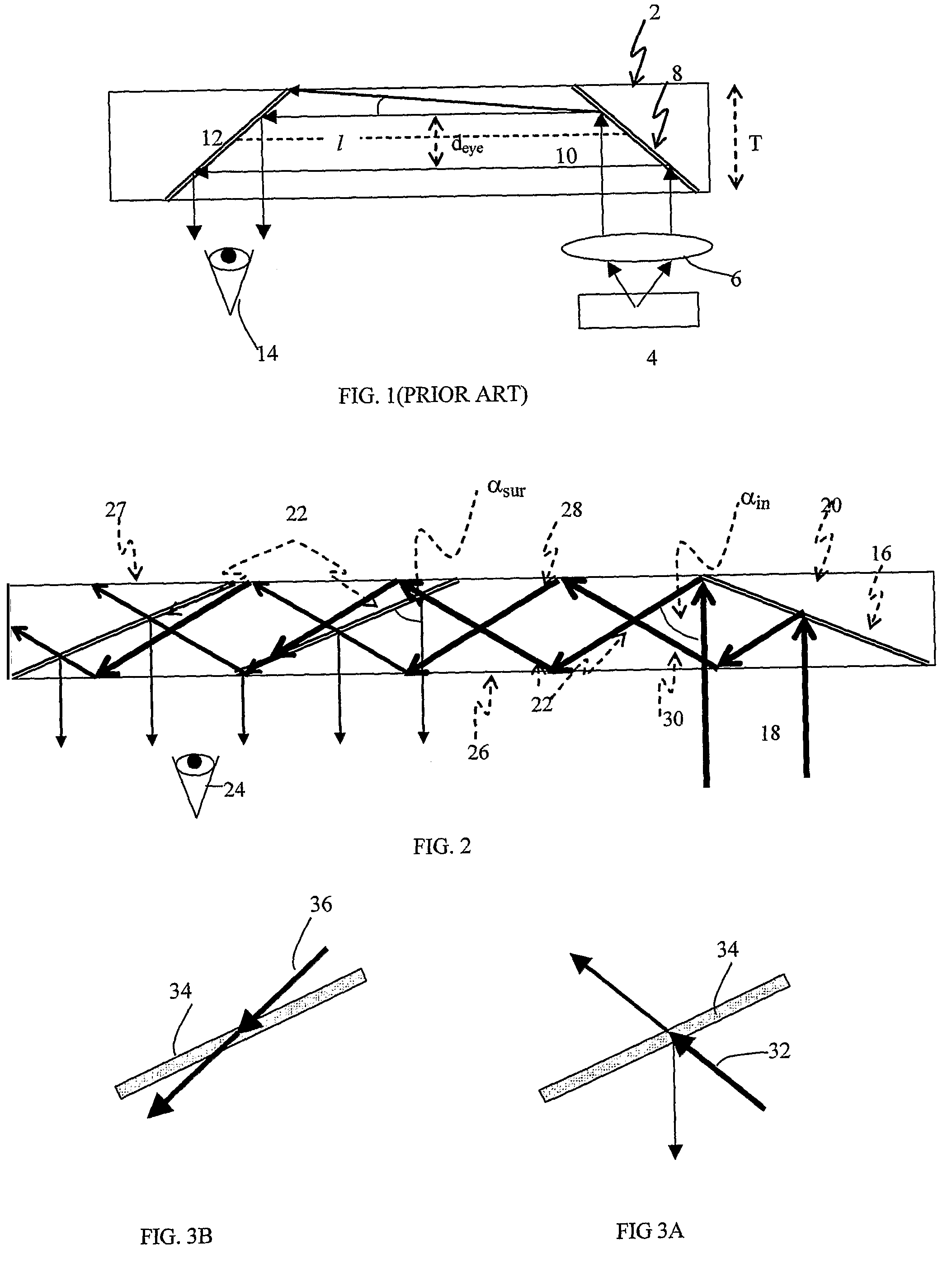
[0039]FIG. 1 illustrates a prior art folding optics arrangement, wherein the substrate 2 is illuminated by a display source 4. The display is collimated by a collimating lens 6. The light from the display source 4 is coupled into substrate 2 by a first reflecting surface 8, in such a way that the main ray 10 is parallel to the substrate plane. A second reflecting surface 12 couples the light out of the substrate and into the eye 14 of a viewer. Despite the compactness of this configuration, it suffers significant drawbacks; in particular only a very limited FOV can be affected. As shown in FIG. 1, the maximum allowed off-axis angle inside the substrate is:
[0040]αmax=arctan(T-deye2l),(1)
wherein T is the substrate thickness;
[0041]deye is the desired exit-pupil diameter, and
[0042]l is the distance between reflecting surfaces 8 and 12.
[0043]With angles higher than αmax the rays are reflected from the substrate surface before arriving at the reflecting surface 12. Hence, the reflect...
PUM
 Abstract
Description
Claims
Application Information