Substrate for a display device and method of manufacturing the same

a display device and substrate technology, applied in the field of substrates for display devices, can solve the problems of static electricity accumulated electric charge flowing through array test pads, reducing manufacturing yield, and damage to lines and thin-film transistors formed on array substrates, so as to reduce static electricity damage or prevent damage, simplify manufacturing process, and simple structure

Active Publication Date: 2013-08-27
SAMSUNG DISPLAY CO LTD
View PDF6 Cites 3 Cited by
  • Summary
  • Abstract
  • Description
  • Claims
  • Application Information

AI Technical Summary

Benefits of technology

[0008]Exemplary embodiments of the present invention provide a mother substrate for a display device that reduces or prevents damage due to static electricity.
[0014]According to some exemplary embodiments of the present invention, an electrostatic preventing pattern having a simple structure is included and damage due to static electricity may be reduced or prevented and a manufacturing process may be simplified.

Problems solved by technology

During the array test process, an accumulated electric charge of static electricity may flow through the array test pads and the lines and the thin-film transistors that are formed on the array substrate may be damaged.
Therefore, the static electricity may cause a decrease in manufacturing yield and a poor quality of products.

Method used


Image

  • Substrate for a display device and method of manufacturing the same
  • Substrate for a display device and method of manufacturing the same
  • Substrate for a display device and method of manufacturing the same

Examples


Embodiment Construction

[0026]Exemplary embodiments of the present invention are described more fully hereinafter with reference to the accompanying drawings. The present invention may, however, be embodied in many different forms and should not be construed as limited to the exemplary embodiments set forth herein. In the drawings, the sizes and relative sizes of layers and regions may be exaggerated for clarity.

[0027]It will be understood that when an element or layer is referred to as being “on,”“connected to” or “coupled to” another element or layer, it can be directly on, connected or coupled to the other element or layer or intervening elements or layers may be present.

[0028]Hereinafter, exemplary embodiments of the present invention will be explained in detail with reference to the accompanying drawings.

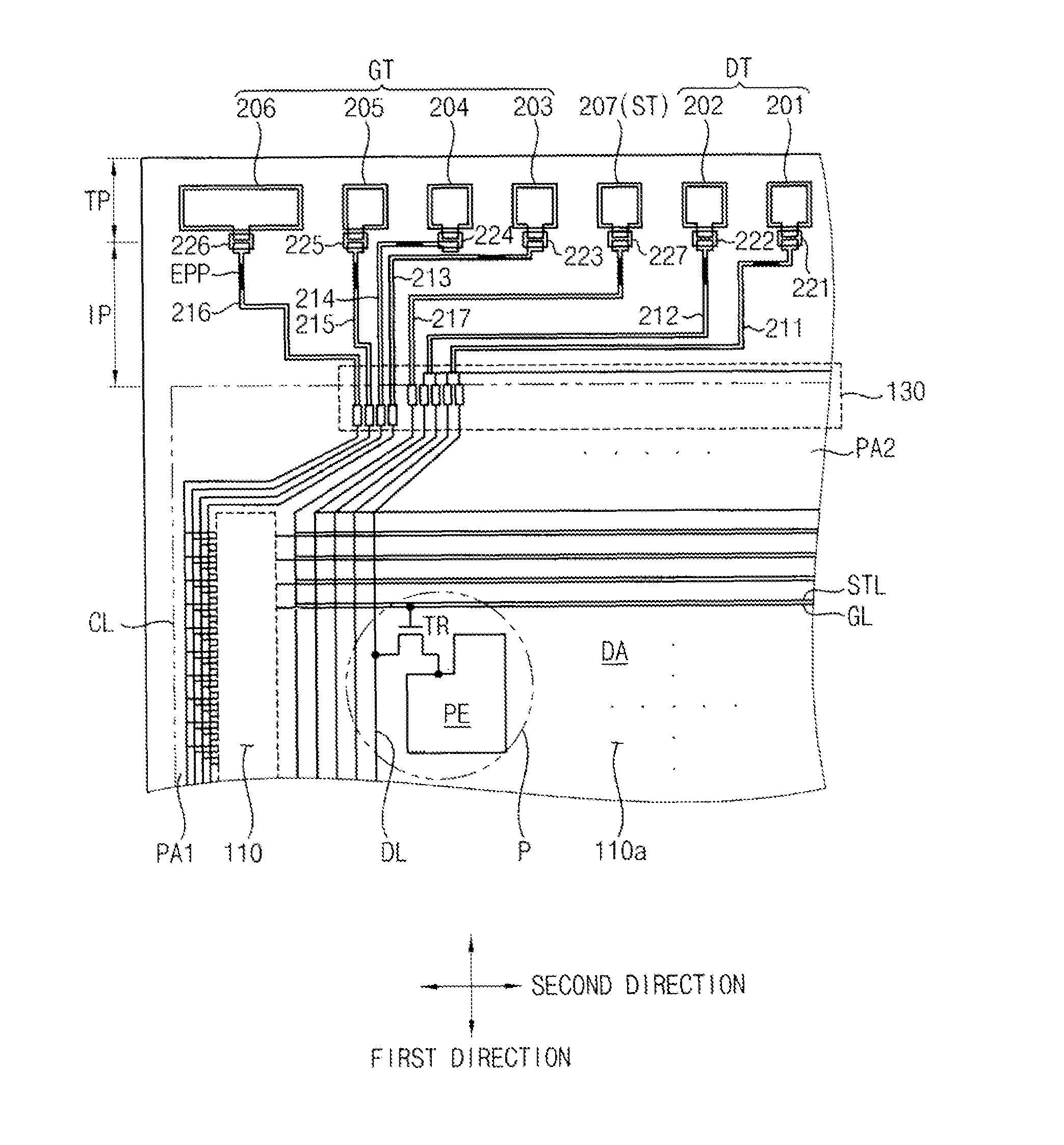
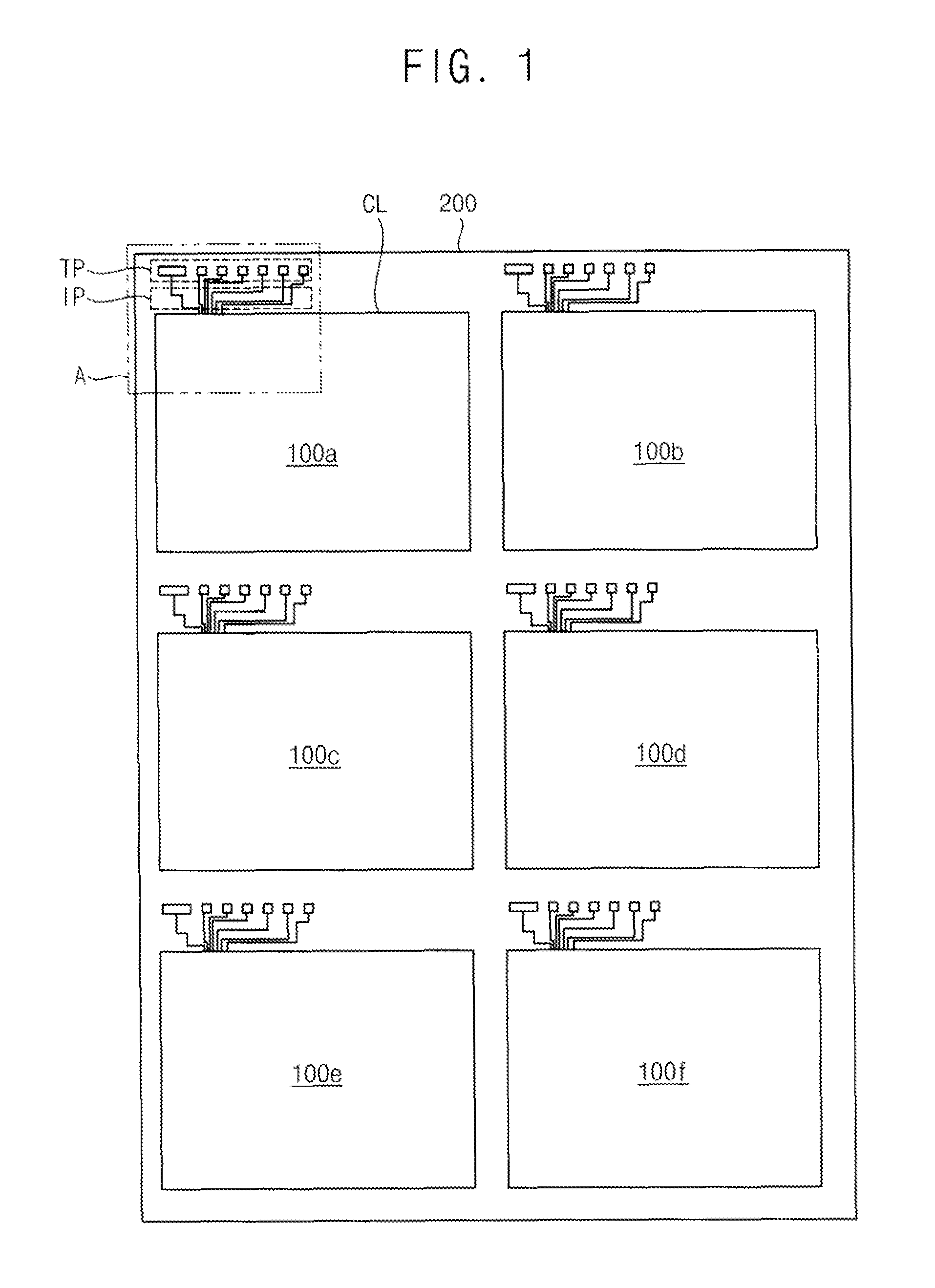
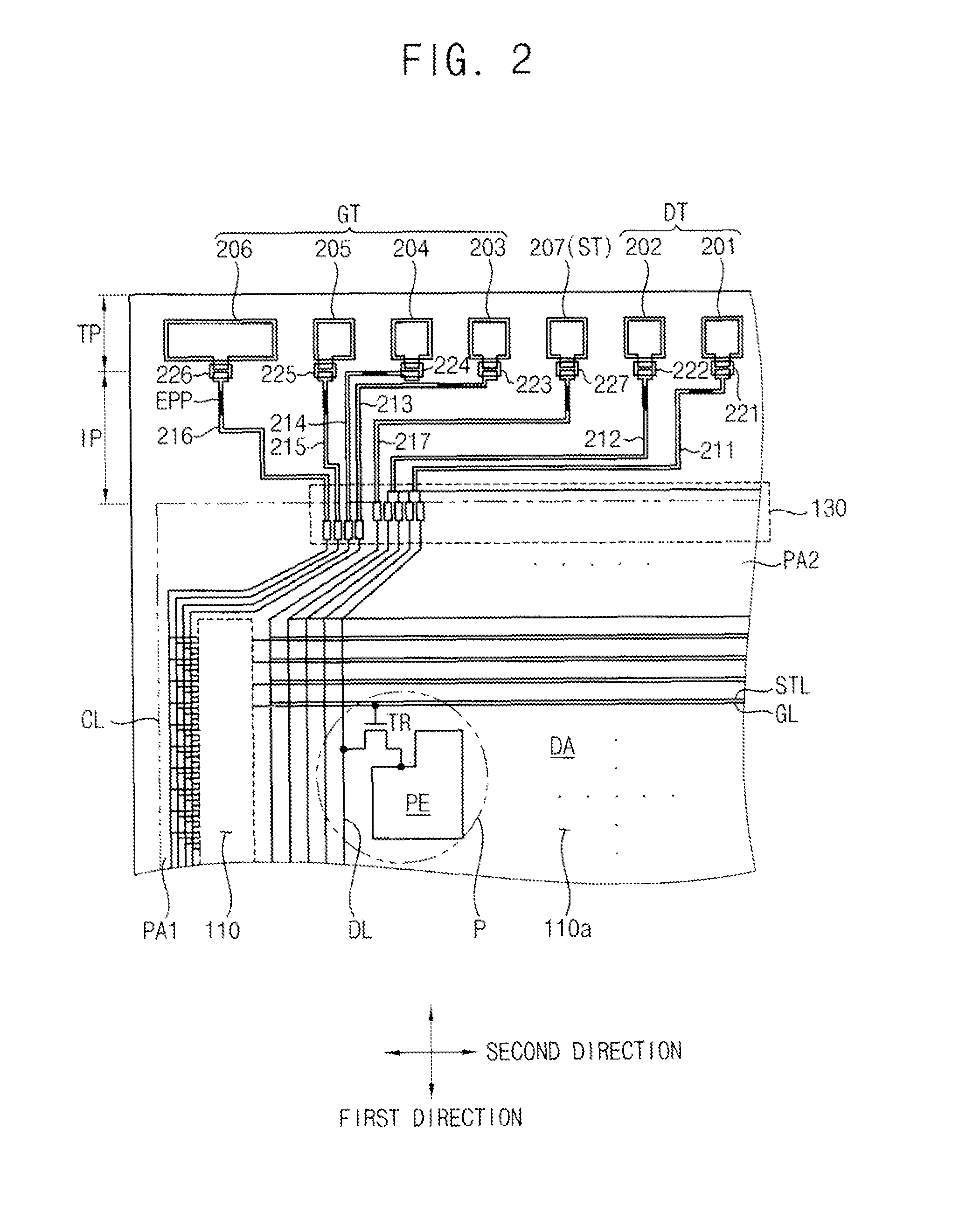
[0029]FIG. 1 is a plan view illustrating a mother substrate according to an exemplary embodiment of the present invention. FIG. 2 is an enlarged view of a portion “A” of the mother substrate of FIG. 1...


PUM

PropertyMeasurementUnit
widthaaaaaaaaaa
widthaaaaaaaaaa
widthaaaaaaaaaa

Abstract

A mother substrate for a display device includes a display cell, a test pad, an electrostatic preventing pattern and a connecting line. The display cell includes a pad and a signal line. The signal line is extended from the pad and is electrically connected to a pixel. The test pad is disposed out of the display cell and is electrically connected to the signal line of the display cell and receives a test signal. The electrostatic preventing pattern electrically connected to the test pad is disposed adjacent to the test pad and includes a plurality of edges. The electrostatic preventing pattern is formed from a metal pattern. The connecting line is extended from the electrostatic preventing pattern and is electrically connected to the pad of the display cell.

Description

CROSS REFERENCE TO RELATED APPLICATION[0001]This application claims priority under 35 U.S.C. §119 to Korean Patent Application No. 10-2009-0101528, filed on Oct. 26, 2009 in the Korean Intellectual Property Office (KIPO), the contents of which are herein incorporated by reference in their entirety.BACKGROUND OF THE INVENTION[0002]1. Technical Field[0003]The present invention relates to a display device. More particularly, the present invention relates to a substrate for a display device and a method of manufacturing the substrate.[0004]2. Discussion of the Related Art[0005]Generally, a liquid crystal display (LCD) panel includes an array substrate, an upper substrate facing the array substrate, and a liquid crystal layer interposed between the array substrate and the upper substrate. The array substrate includes a display area in which a plurality of lines and a plurality of thin-film transistors connected to the lines are formed, and a peripheral area in which pads applying an elec...

Claims


Application Information

Patent Timeline
Patent Type & Authority Patents(United States)
IPC IPC(8): G02F1/1333G02F1/1345
CPCG02F1/1345H01L22/14H05F1/00G02F1/1309G02F1/133351G02F2202/22H01L2924/0002H01L2924/00
Inventor LEE, MI-SUNKANG, SHIN-TACK
Owner SAMSUNG DISPLAY CO LTD
Why Eureka
Try Eureka