Multilayer ceramic electronic component, series of electronic components stored in a tape, and method of manufacturing multilayer ceramic electronic component

a technology of multi-layer ceramic and electronic components, which is applied in the direction of capacitor manufacturing, fixed capacitor details, printed circuit non-printed electric components association, etc., can solve the problems of increasing the probability of the main body of the multi-layer ceramic electronic component becoming damaged, and the damage of the multi-layer ceramic electronic component at the time of mounting so as to achieve significant reduction or prevention of damage to the multi-layer ceramic electronic component. , the effect of reducing the damag

Active Publication Date: 2015-09-08
MURATA MFG CO LTD
View PDF2 Cites 0 Cited by
  • Summary
  • Abstract
  • Description
  • Claims
  • Application Information

AI Technical Summary

Benefits of technology

[0006]Accordingly, preferred embodiments of the present invention significantly reduces or prevents damage to a multilayer ceramic electronic component at the time of mounting the multilayer ceramic electronic component.
[0012]In various preferred embodiments of the present invention, damage to a multilayer ceramic electronic component at the time of mounting the multilayer ceramic electronic component is significantly reduced or prevented.

Problems solved by technology

When a multilayer ceramic electronic component is mounted on a mounting substrate, the multilayer ceramic electronic component may sometimes become damaged.
In particular, in the case where a protruding portion is present on a main surface of a multilayer ceramic electronic component, when the multilayer ceramic electronic component is mounted on a mounting substrate in such a manner that the main surface of the multilayer ceramic electronic component on which the protruding portion is present and the mounting substrate face each other, a stress is concentrated at an interface between outer electrodes and a main body of the multilayer ceramic electronic component while the protruding portion serves as a fulcrum, and as a result, the probability of the main body of the multilayer ceramic electronic component becoming damaged increases.

Method used


Image

  • Multilayer ceramic electronic component, series of electronic components stored in a tape, and method of manufacturing multilayer ceramic electronic component
  • Multilayer ceramic electronic component, series of electronic components stored in a tape, and method of manufacturing multilayer ceramic electronic component
  • Multilayer ceramic electronic component, series of electronic components stored in a tape, and method of manufacturing multilayer ceramic electronic component

Examples


Embodiment Construction

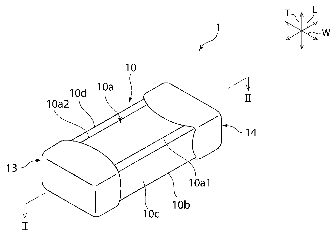
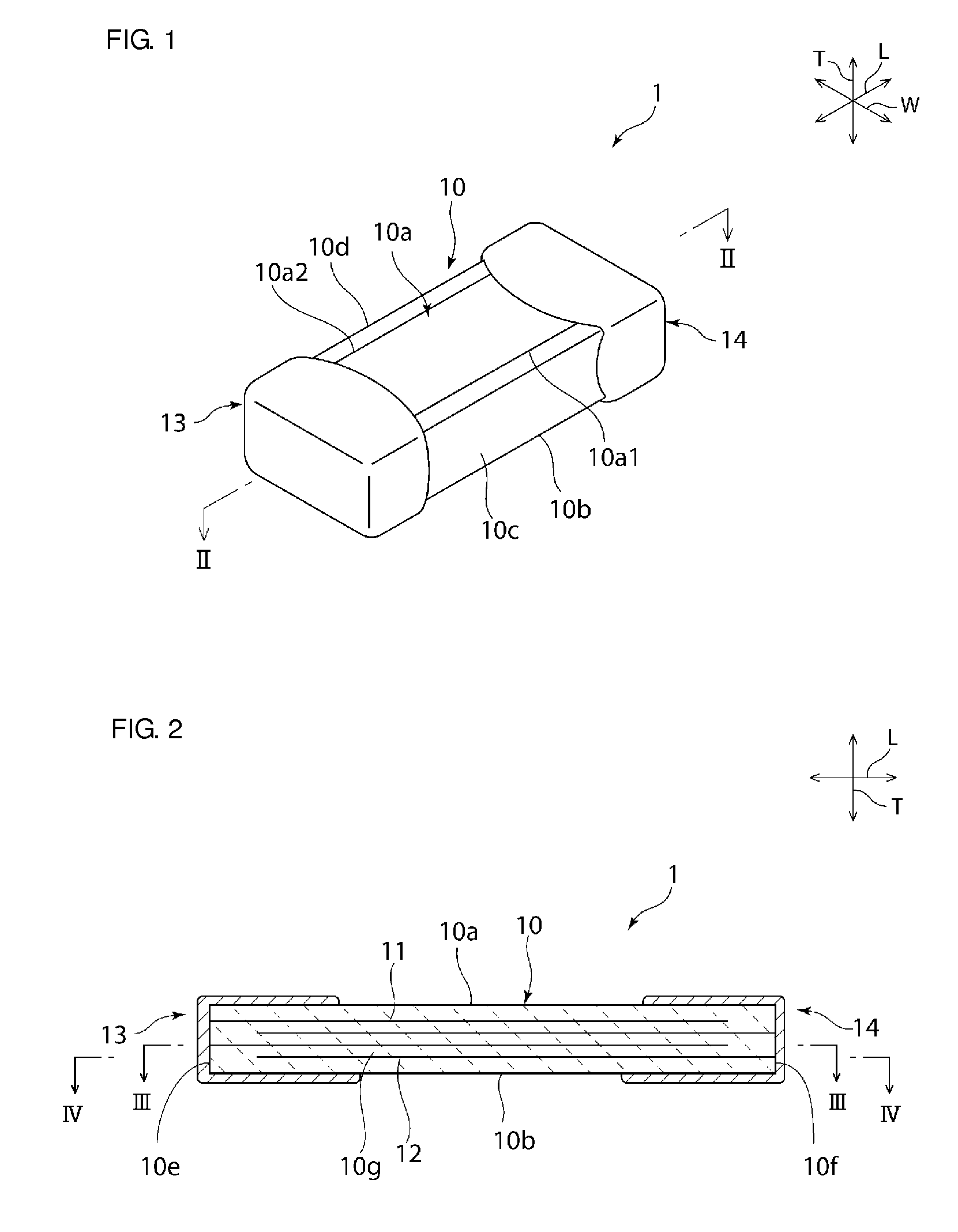
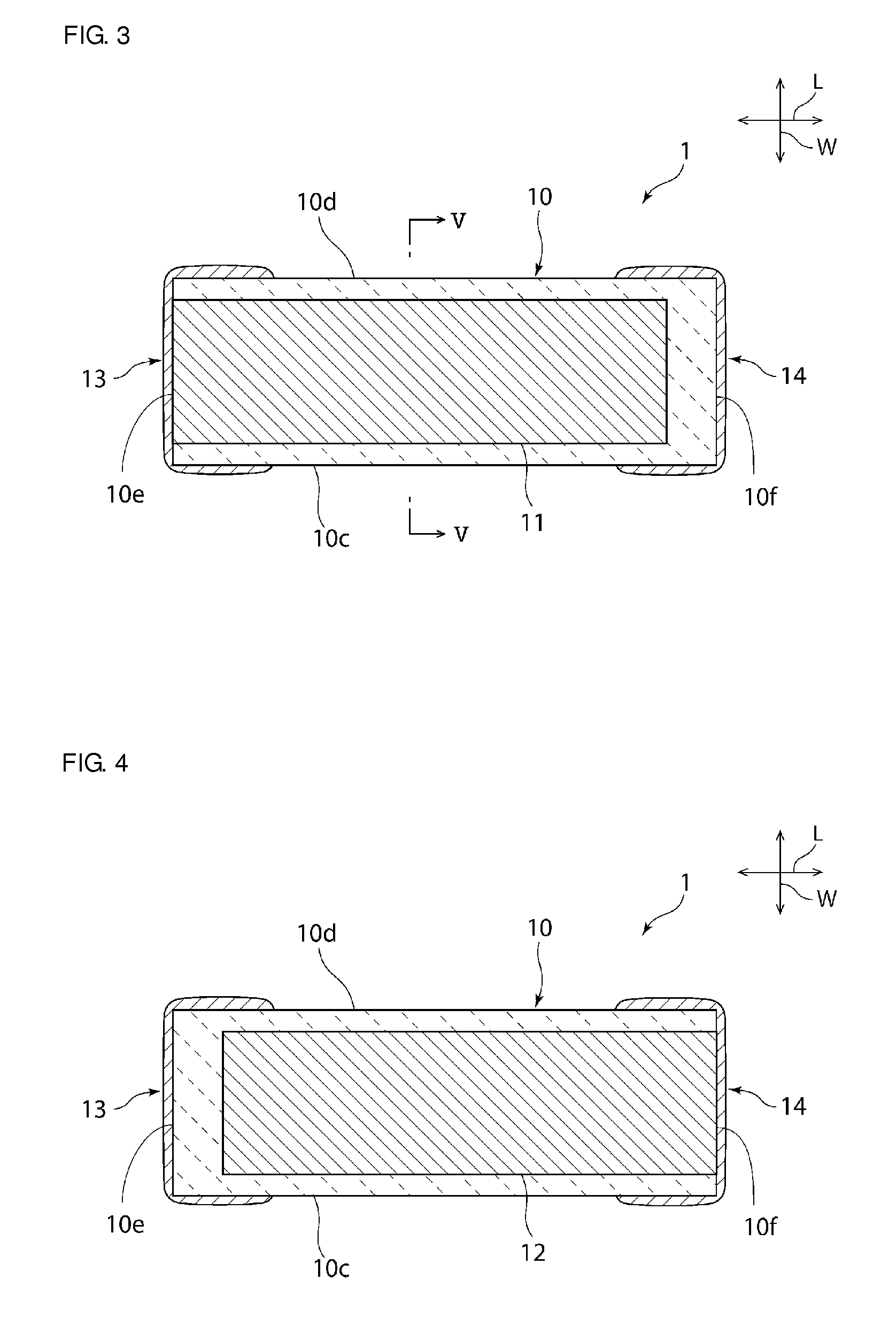
[0023]Examples of preferred embodiments of the present invention will be described below. However, the following preferred embodiments are merely examples. The present invention is in no way limited to the following preferred embodiments.

[0024]In the drawings that will be referred to in the description of the preferred embodiments and so forth, members that have the same or substantially the same functions are referred to by the same reference numerals. In addition, the drawings that will be referred to in the description of preferred embodiments and so forth are schematically illustrated. Dimensional ratios and so forth of objects that are illustrated in the drawings may sometimes be different from dimensional ratios and so forth of actual objects. The dimensional ratios and so forth of the objects may also sometimes differ between the drawings. The specific dimensional ratios and so forth of the objects should be determined by taking the following description into consideration.

[0...


PUM

PropertyMeasurementUnit
lengthaaaaaaaaaa
widthaaaaaaaaaa
thicknessaaaaaaaaaa

Abstract

In a multilayer ceramic electronic component, a size of a step portion on a first main surface and a size of a step portion on a second main surface are different from each other. A first outer electrode includes a plating film containing Cu. A length of a portion of the plating film containing Cu that is positioned on the first main surface in a length direction and a length of a portion of the plating film containing Cu that is positioned on the second main surface in the length direction are different from each other.

Description

BACKGROUND OF THE INVENTION[0001]1. Field of the Invention[0002]The present invention relates to a multilayer ceramic electronic component, a series of electronic components stored in a tape, and a method of manufacturing a multilayer ceramic electronic component.[0003]2. Description of the Related Art[0004]In the related art, a multilayer ceramic electronic component that includes first inner electrodes and second inner electrodes that are alternately disposed in a thickness direction has been used in various devices. In such a multilayer ceramic electronic component, the first and second inner electrodes are not disposed across the entire multilayer ceramic electronic component. Thus, there is a difference in thickness between a portion in which the first and second inner electrodes are disposed and the other portions. A protruding portion is generally formed on one main surface of the multilayer ceramic electronic component due to the difference in thickness (see, for example, Ja...

Claims


Application Information

Patent Timeline
Patent Type & Authority Patents(United States)
IPC IPC(8): H05K1/18H01G4/12H01G4/248H01F27/28H01F5/00H01C7/00H01C1/148H01C17/00H01L41/22H01F41/32H01G13/00H01G4/012H01G4/30H01L41/047
CPCH05K1/185H01C1/148H01C7/008H01C17/00H01F5/00H01F27/2804H01F41/32H01G4/012H01G4/1209H01G4/248H01G4/30H01G13/00H01L41/0472H01L41/0477H01L41/22H01F2027/2809H01G4/232H01F17/0013H01F27/292H10N30/872H10N30/877H10N30/063H10N30/01
Inventor SHIMIZU, KOTARO
Owner MURATA MFG CO LTD
Why Eureka
Try Eureka