Display method of display device

a display device and display method technology, applied in the field of display methods of display devices, can solve the problems of stymied power loss cut, follow high-speed operation, and leakage of signals written into pixel data even in the off sta

Inactive Publication Date: 2015-02-03
SEMICON ENERGY LAB CO LTD
View PDF152 Cites 3 Cited by
  • Summary
  • Abstract
  • Description
  • Claims
  • Application Information

AI Technical Summary

Benefits of technology

[0008]The switching transistor included in the conventional active matrix display device has a drawback in that the off-state current is high and thus a signal written into a pixel leaks to be lost even in the off state. Although such a drawback does not matter in the case of displaying a moving image, frequent signal rewriting into pixels is needed even in the case of keeping displaying the same image such as a still image, which stymies cut of power loss.
[0009]In view of the above, a method for reducing power consumption in which a display element having memory properties is applied to the active matrix display device has been used. However, many of the display elements having memory properties have drawbacks of low operation speed, and thus, they cannot follow high-speed operation of the switching transistor provided in the pixel and it is difficult to display a moving image.
[0010]Further, in display devices for displaying both a moving image and a still image, a display device which enables both moving image display and low power consumption, using, for example, a method for controlling the frequency of signal writings into a pixel in accordance with the display image characteristics has been demanded.
[0023]According to the present invention, a display method suitable for an image provided by a digital data file can be provided. Further, a display method of a display device, for adjusting the image quality and power consumption to display an image in accordance with the state of the display device or at user's request can be provided.

Problems solved by technology

The switching transistor included in the conventional active matrix display device has a drawback in that the off-state current is high and thus a signal written into a pixel leaks to be lost even in the off state.
Although such a drawback does not matter in the case of displaying a moving image, frequent signal rewriting into pixels is needed even in the case of keeping displaying the same image such as a still image, which stymies cut of power loss.
However, many of the display elements having memory properties have drawbacks of low operation speed, and thus, they cannot follow high-speed operation of the switching transistor provided in the pixel and it is difficult to display a moving image.
However, a variety of formats have been used for the digital data file, which makes it quite difficult for users to select a display method accordingly.

Method used


Image

  • Display method of display device
  • Display method of display device
  • Display method of display device

Examples


embodiment 1

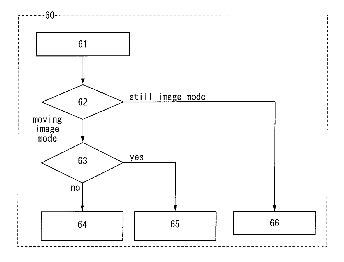
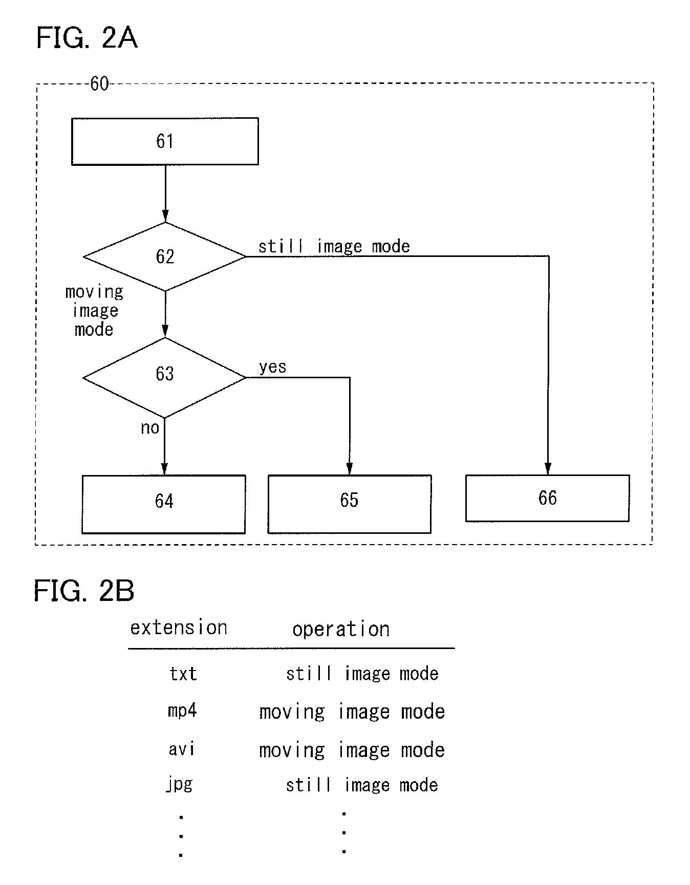
[0036]In Embodiment 1, a structure and a method of a display device in which an operation of the display device is decided in accordance with the kind of an image which is provided by a digital data file and the image is displayed will be described using FIG. 1, FIGS. 2A and 2B, FIG. 3, FIG. 4, FIGS. 5A and 5B, and FIG. 6.

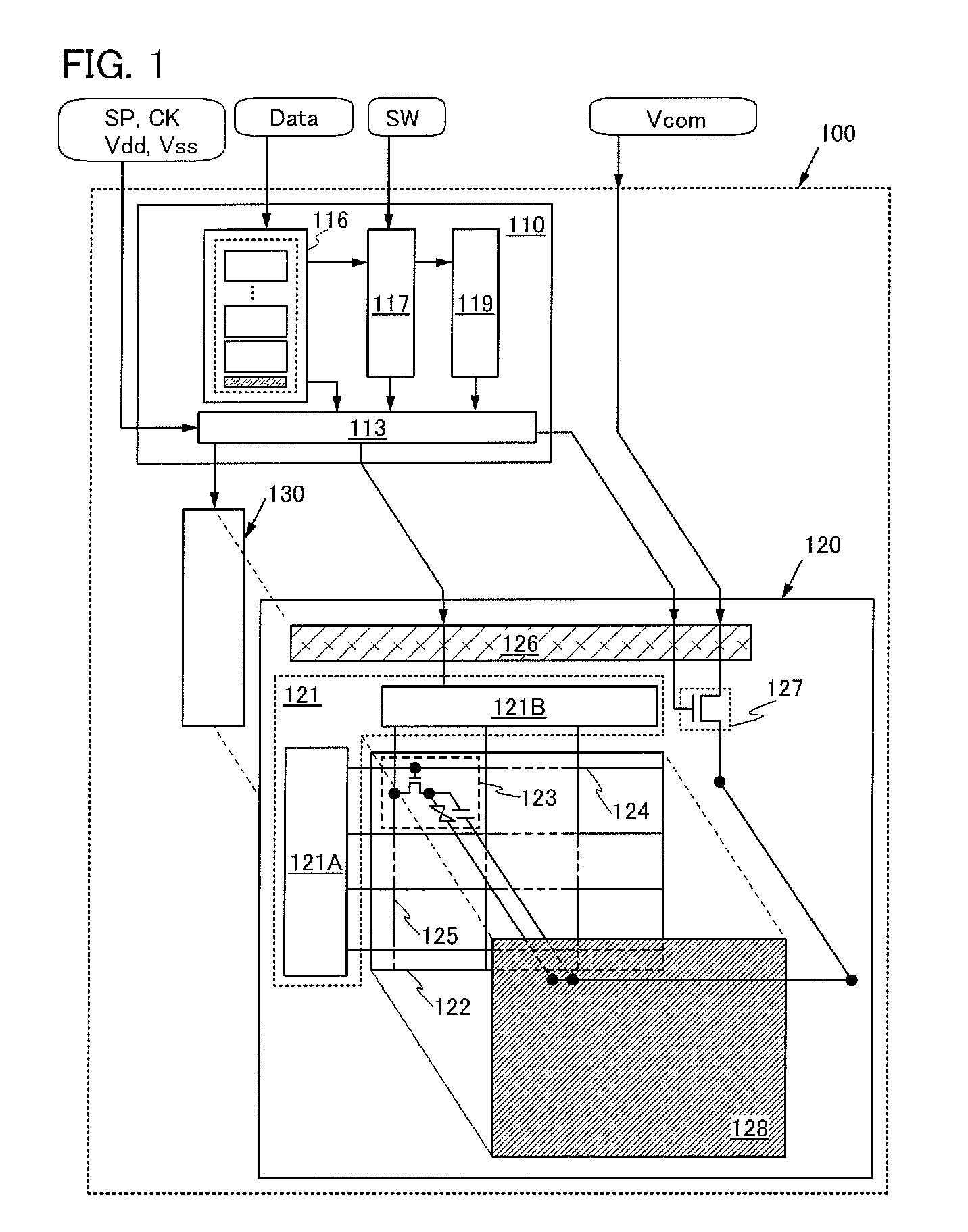
[0037]Each structure of a display device 100 according to one embodiment of this description is described using a block diagram of FIG. 1. The display device 100 of this embodiment includes an image processing circuit 110, a display panel 120, and a lighting unit 130.

[0038]A control signal, a digital data file, and a power supply potential are supplied to the display device 100 of this embodiment from an external device. A start pulse SP and a clock signal CK are supplied as control signals, and a high power supply potential Vdd, a low power supply potential Vss, and a common potential Vcom are supplied as power supply potentials. Further, an image and data which i...

embodiment 2

[0106]Described in Embodiment 2 is a method for displaying an image provided by a digital data file on a display device in which a switching element whose off-state current is reduced is provided in a pixel, using data correlated to an operation of the display device, which is provided by the digital data file. In particular, a standard play mode of a moving image and a simple play mode in which the frequency of refreshings of a display panel is reduced are described below using FIGS. 3 and 7.

[0107]In this embodiment, an example in which the data correlated to an operation of the display device is provided by a script file or header data is described.

[0108]The composition of a digital data file applied to the display device described in this embodiment is described below. The digital data file used in this embodiment contains a frame compressed in the format decodable independently from the preceding and following frames. Examples of such a format of a digital data file are MPEG2, M...

embodiment 3

[0134]In Embodiment 3, one example of a transistor which can be applied to the display device disclosed in this description and the like will be described. There is no particular limitation on a structure of the transistor which can be applied to a display device disclosed in this description and the like; for example, a top-gate structure or a bottom-gate structure such as a staggered type or a planar type can be used. Further, the transistor may have a single gate structure including one channel formation region, a double gate structure including two channel formation regions, or a triple gate structure including three channel formation regions. Alternatively, the transistor may have a dual gate structure including two gate electrode layers positioned over and below a channel region with a gate insulating layer provided therebetween. Note that examples of a cross-sectional structure of a transistor illustrated FIGS. 8A to 8D are described below. Transistors illustrated in FIGS. 8A...


PUM


Abstract

A display method suitable for an image provided by a digital data file and / or a display method of a display device in which the image quality and power consumption are adjusted in accordance with the state of the display device or at user's request to display an image. The image is displayed on the display device in which a plurality of pixels having a pixel electrode connected to a switching element whose off-state current is reduced, using the image provided by the digital data file and data which is provided by the digital data file and is correlated to an operation of the display device.

Description

TECHNICAL FIELD[0001]The present invention relates to a display method of a display device, using a file including data for controlling the display device.BACKGROUND ART[0002]There have been active matrix display devices in which a plurality of pixels is arranged in matrix, and a switching transistor and a display element which is connected to the switching transistor are provided for each pixel.[0003]As a switching transistor preferable for the active matrix display device, a transistor including a channel formation region including metal oxide has drawn attention (Patent Documents 1 and 2). Further, as examples of a display element applicable to the active matrix display device, a liquid crystal element, electronic ink using an electrophoresis method, and the like can be given.[0004]Active matrix display devices using liquid crystal elements have been used in wide application from moving image display taking advantage of high operation speed of the liquid crystal element to still ...

Claims


Application Information

Patent Timeline
Patent Type & Authority Patents(United States)
IPC IPC(8): G09G5/00G09G3/36
CPCG09G3/3648G09G3/3655G09G2320/10G09G2330/021G09G2340/02G09G2340/0435
Inventor WAKIMOTO, KENICHIHAYAKAWA, MASAHIKO
Owner SEMICON ENERGY LAB CO LTD
Why Eureka
Try Eureka