
Nano graphical and ultrawide-band electromagnetic property measuring system
A technology of electromagnetic characteristics and nano-patterns, applied in the fields of electromagnetic field characteristics, radio-frequency circuit testing, and measuring devices, can solve the problems of difficult patterning process, cumbersome processing and measurement process, prolonging the testing time of nano-materials and devices, etc., to achieve Extensive application fields and market demands, rapid and efficient testing and research results
Patent Information
- Authority / Receiving Office
- CN · China
- Patent Type
- Applications(China)
- Current Assignee / Owner
- Publication Date
- 2013-01-30
Smart Images
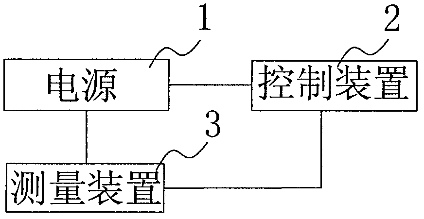
Figure 1 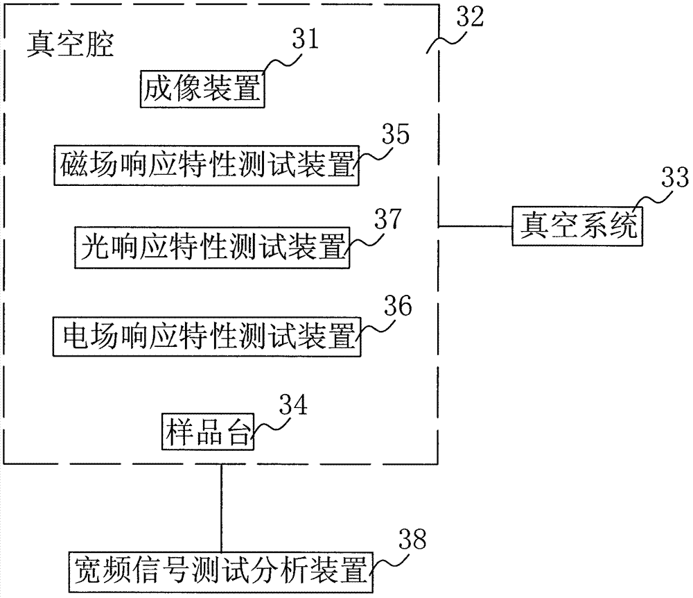
Figure 2 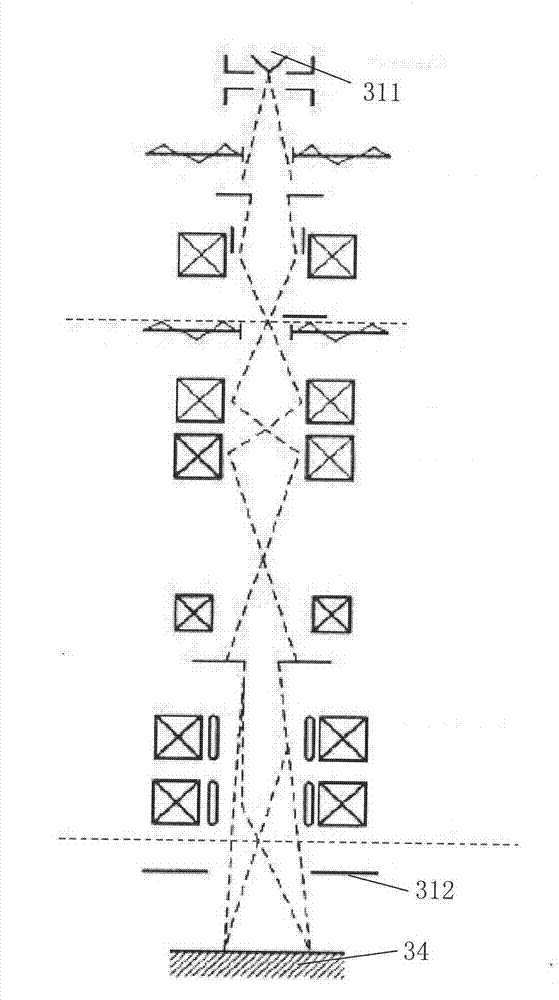
Figure 3
Abstract
Description
technical field
[0001] The invention relates to a detection device for nanomaterials and devices, especially a magnetic field application based on an electron beam exposure system / electron beam pattern generation system, high-frequency electromagnetic signal generation, introduction, transmission and measurement, and nano-positioning in a large range Nanopatterning and ultra-wideband electromagnetic characteristic measurement system. Background technique
[0002] With the development of nano-processing and detection technology, nano-materials and devices have been widely used in many fields including electronics, magnetism, chemistry, and biology. Research on nanomaterials and devices has become one of the core issues in condensed matter physics, modern information technology and industrial production. Since 1988, the rapid development of spintronics is gradually bringing information science into an era of extremely high-density magnetic storage (T-bit / inch2) including nano...
Examples
Embodiment Construction
[0085] Below in conjunction with accompanying drawing, structural principle and working principle of the present invention are specifically described:
[0086] The invention introduces the measuring magnetic field to the sample stage with the function of SEM imaging or EBL patterning, so as to realize the test of the magnetic field response characteristic of the tested nanometer material or device. see figure 1 , figure 2 and image 3 , figure 1 It is a structural block diagram of the present invention, figure 2 It is a structural block diagram of a measuring device according to an embodiment of the present invention, image 3 It is a working principle diagram of the imaging device of the present invention. The nano-patterning and ultra-broadband electromagnetic characteristic measurement system of the present invention includes a power supply 1, a control device 2 and a measurement device 3, the control device 2 is connected to the measurement device 3, the control dev...