
Handling method for epitaxy defect
A technology of epitaxial defects and processing methods, which is applied in the field of epitaxial defect processing, can solve the problems of increased internal leakage of devices, reduced internal quantum efficiency, and deterioration of fill factor open circuit voltage performance, so as to reduce leakage and non-radiative recombination Effect
Patent Information
- Authority / Receiving Office
- CN · China
- Current Assignee / Owner
- Publication Date
- 2016-10-12
- Estimated Expiration
- Not applicable · inactive patent
Smart Images
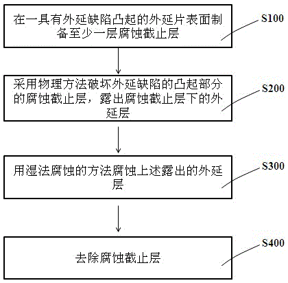
Figure 1 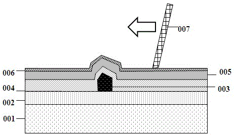
Figure 2 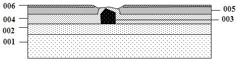
Figure 3
Abstract
Description
technical field
[0001] The invention relates to a method for processing epitaxial defects, belonging to the technical field of semiconductor devices and processes. Background technique
[0002] Chemical vapor deposition methods such as metal-organic chemical vapor deposition (MOCVD) are widely used in LEDs and multi-junction solar cells. The epitaxial layers of both LEDs and multi-junction solar cells consist of multiple thin layers. With the most mature Ge / In 0.01 GaAs / GaInP triple-junction cells are taken as an example. The epitaxial process is to grow In on a Ge substrate by MOCVD. 0.01 For the GaAs middle cell and the GaInP top cell, each junction cell has a multilayer epitaxial structure of window layer, emitter region, base region, and back field layer, and there is a tunnel junction layer between the sub-cells.
[0003] In the process of chemical vapor deposition, it is difficult to ensure absolute cleanliness on the surface of the epitaxial wafer, and foreign obje...
Examples
Embodiment Construction
[0029] The present invention will be further described below in conjunction with the examples, but the protection scope of the present invention should not be limited thereby.
[0030] The following embodiment discloses a processing method for epitaxial defects caused by epitaxial dropout phenomenon, please refer to figure 1 , which mainly includes steps S100~S400, first forming an etch stop layer on the surface of the epitaxial layer, then combining physical and chemical methods, using physical methods to destroy the etch stop layer of the raised part of the epitaxial defect, in the chemical wet etching process The corrosion stop layer only protects the epitaxial layer other than the raised position, and realizes the selective etching and passivation of the epitaxial layer at the raised defect position.
[0031] Taking a multi-junction solar cell as an example, the method for manufacturing a semiconductor device using the above processing method will be described in detail be...