
Data reception device
a data reception and data technology, applied in the field of data reception devices, can solve the problems of increasing cost, affecting the operation speed of liquid crystal panel modules, and affecting the operation speed of the system, so as to achieve high speed operation, low power consumption, and low cost
Patent Information
- Authority / Receiving Office
- US · United States
- Patent Type
- Patents(United States)
- Current Assignee / Owner
- Publication Date
- 2018-06-26
Smart Images
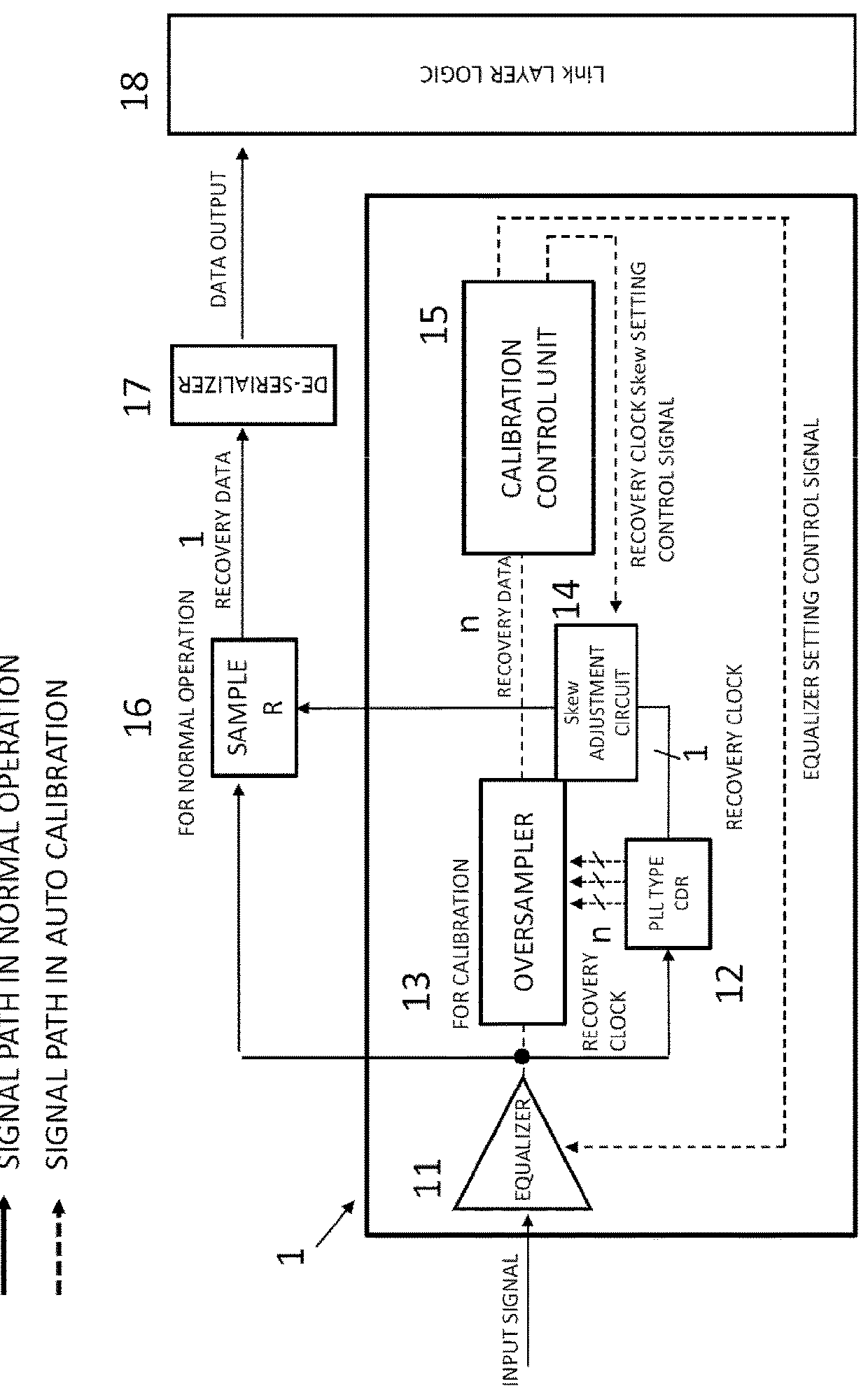
Figure 1 
Figure 2 
Figure 3
Abstract
Description
BACKGROUND
[0001] Technical Field
[0002] The present invention relates to a data reception device in an interface for transmitting image data to a liquid crystal panel module at high speed.
[0003] Related Art
[0004] In a market for mobile devices such as laptop PC and tablet PC, there always is a request for reduction in power consumption and cost. Meanwhile, a data processing amount and an operating frequency have steadily increased along with improvement of resolution of a panel and improvement of image quality of a display, and the reduction of the power consumption and the cost reduction have become major problems which conflict thereto.
[0005] As flow of drawing data to the panel in the laptop PC or the tablet PC, it is configured to use a processor such as a central processing unit (CPU) and a graphics processing unit (GPU) that are in charge of calculation of the drawing data itself, various calculation processing and graphics processing, a timing controller (TCON) that performs timing...
Examples
first embodiment
[0055][First Embodiment of Present Invention]
[0056]A first embodiment of the present invention will be described. FIG. 1 is a block diagram for describing an overall configuration of a data receiving circuit 1 according to the present invention. Here, a basic configuration of the data receiving circuit 1 will be described with reference to FIG. 1.
[0057]The data receiving circuit 1 is a circuit incorporated in a timing controller in, for example, a laptop PC or a tablet PC and receives drawing data transmitted from a processor such as a CPU and a GPU. The timing controller is a large-scale integration (LSI) that generates various timing signals so that drawing data transmitted from the processor such as the CPU and the GPU matches a timing of a liquid crystal panel. The interface between the processor and the timing controller conforms to, for example, an eDP standard of VESA. That is, the timing controller receives the drawing data from the processor through a Main-Link (main signal...
second embodiment
[0080][Second Embodiment of Present Invention]
[0081]A second embodiment of the present invention will be described. The second embodiment of the present invention is given as follows. In the first embodiment described above, the gain level of the equalizer circuit can be optimally set in the link training sequence at the time of starting the power supply. However, a power supply level of the IC fluctuates depending on an operation state, and temperature also fluctuates even after the link training is completed and the operation is shifted to the normal operation. Since such fluctuations in the power supply level and temperature affect characteristics of the equalizer circuit as described above, it is desirable to periodically review (calibrate) the optimum value even after shifting to the normal operation. As described above, the contact resistance of the IC mounted on the glass changes with time, and the resistance value may increase in some cases. In view of these phenomena, there...
third embodiment
[0083][Third Embodiment of Present Invention]
[0084]A third embodiment of the present invention will be described. The third embodiment of the present invention is given as follows. As described above, the clock is superimposed on the data line in the high-speed serial interface such as the eDP, and it is necessary to extract the clock synchronized with the data from the serial data input. Therefore, the CDR circuit is the circuit which generates the clock signal synchronized in timing with the data from the serial data input. The CDR circuit is generally configured using the PLL. Although the sampler during the normal operation samples a data signal as output from the equalizer circuit and a clock signal as output from the PLL, a delay from the equalizer circuit to the sampler varies depending on the power supply fluctuations, the temperature fluctuations, and the semiconductor manufacturing variation no matter how carefully a layout is designed. Influence that the delay (timing ske...