
Functional device and production method therefor
a technology of functional devices and production methods, applied in the direction of semiconductor devices, electrical apparatus, layered products, etc., can solve the problems of deteriorating photoelectric conversion efficiency, low doping efficiency, peeling from the interface, etc., to prevent cracks and peeling in the dielectric layer 32, high yield, excellent characteristics
Patent Information
- Authority / Receiving Office
- US · United States
- Patent Type
- Applications(United States)
- Current Assignee / Owner
- Publication Date
- 2004-08-12
- Estimated Expiration
- Not applicable · inactive patent
Smart Images
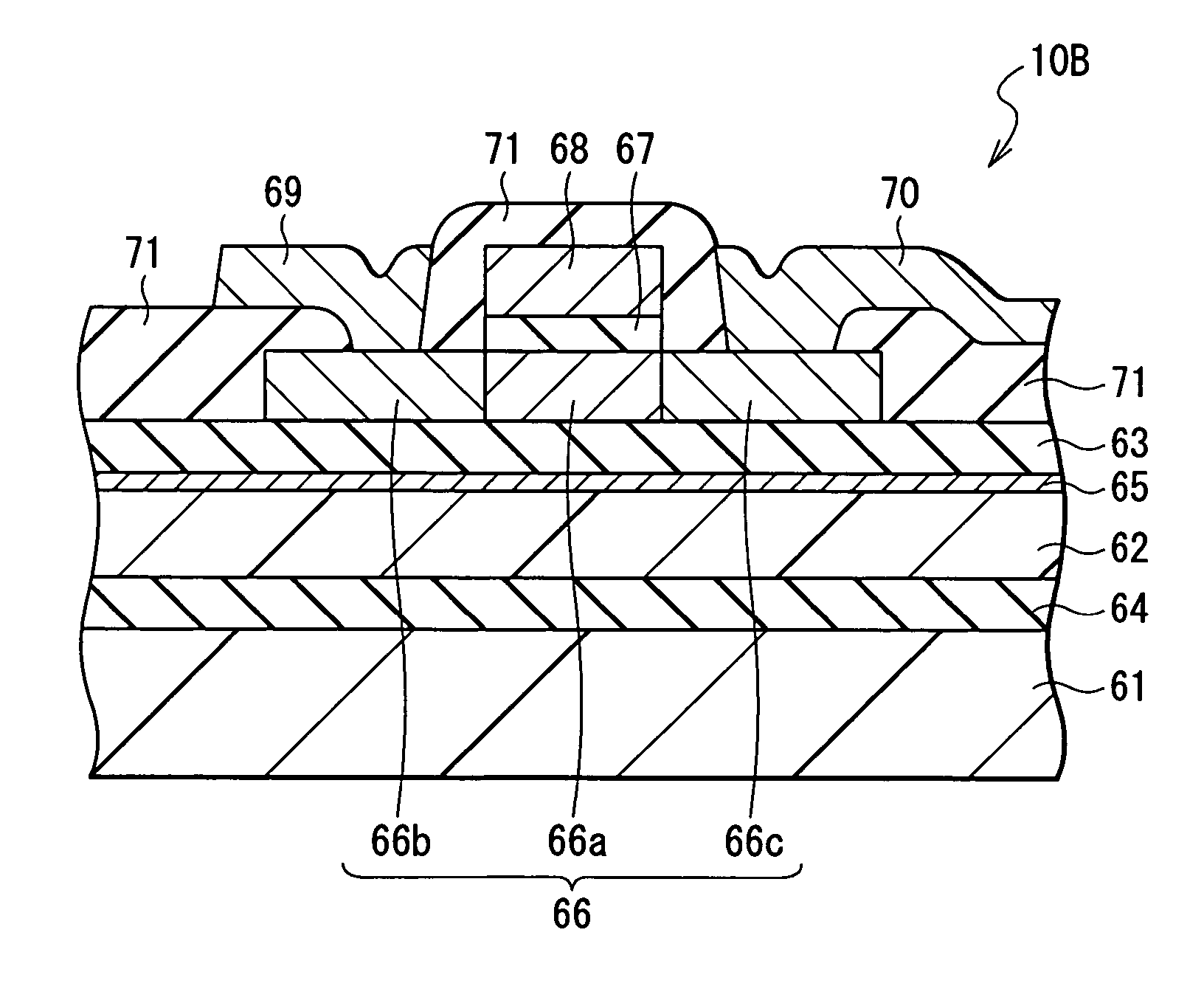
Figure 1 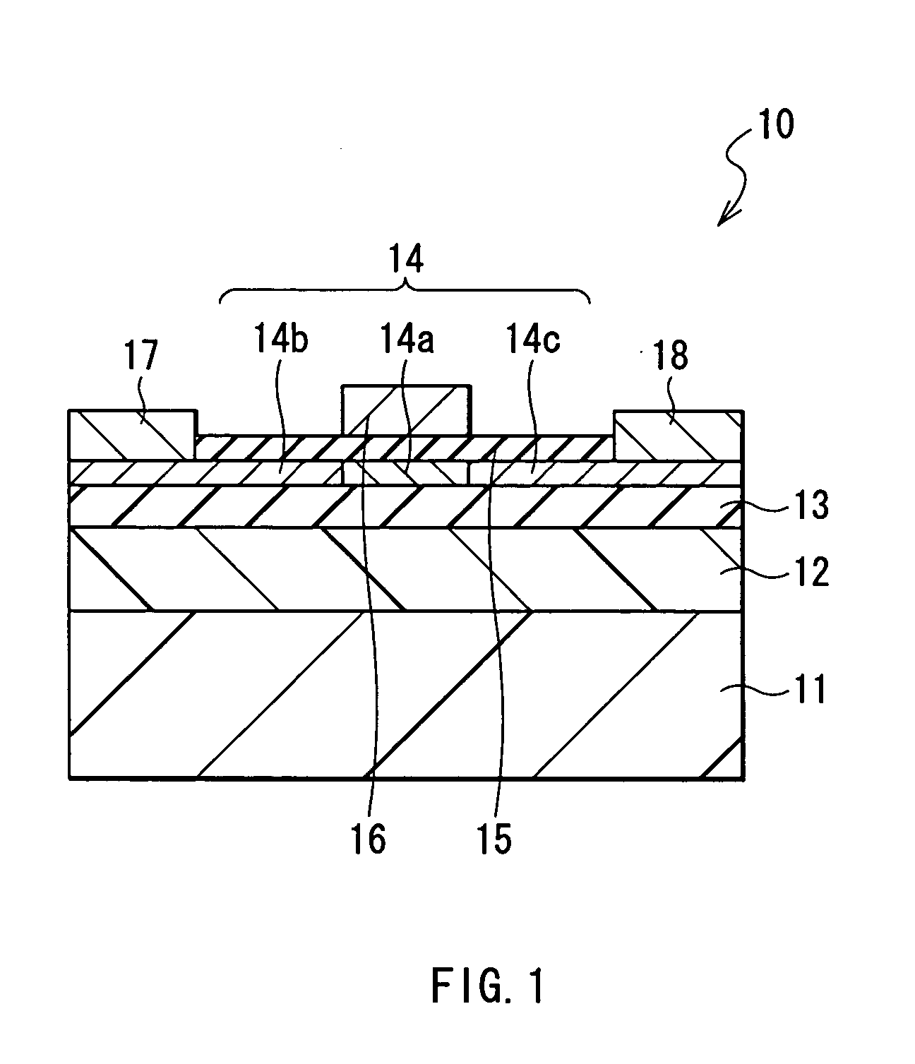
Figure 2 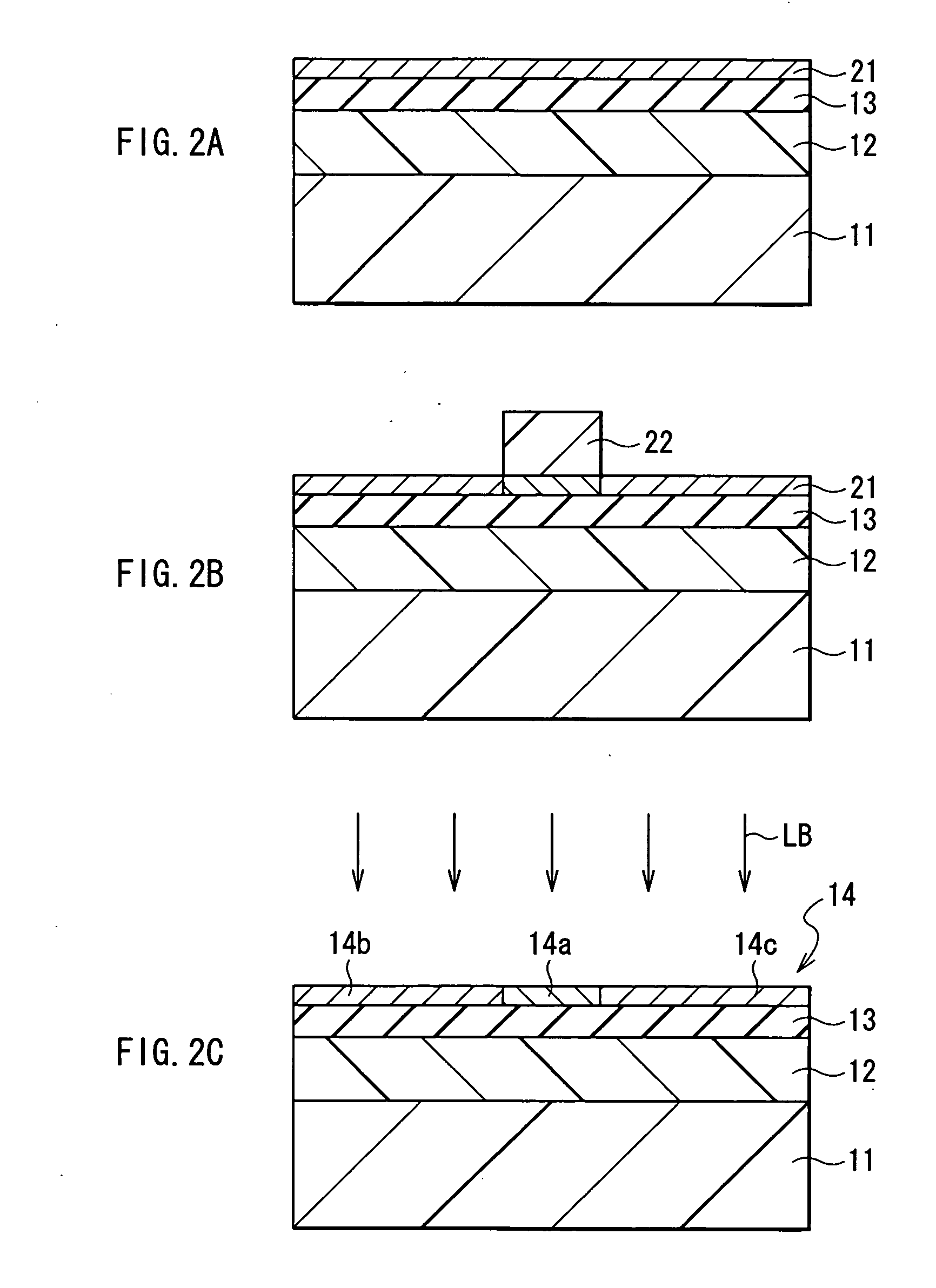
Figure 3
Abstract
Description
[0001] The present invention relates to a functional device having a functional layer, such as a thin film transistor, a dielectric capacitor, or a solar battery, and a method of manufacturing the same.
[0002] Since the pn junction of a hydrogenated amorphous silicon was developed in 1976, the hydrogenated amorphous silicon has been being actively studied. The hydrogenated amorphous silicon has a structure in which a dangling bond in a network made of silicon is terminated by hydrogen or fluorine, and its film can be formed at a low temperature equal to or lower than 300.degree. C. Consequently, the film can be formed on a cheap glass substrate. A study is being made to apply the hydrogenated amorphous silicon to a functional device such as a thin film transistor (TFT), a solar battery, or an optical sensor.
[0003] However, when the hydrogenated amorphous silicon is used as it is, in the case of a TFT, only carrier mobility as low as about 0.1 to 0.5 cm.sup.2 / V*S can be obtained. In t...
Examples
example 2
[0093] In this example, a polysilicon layer was formed in a manner similar to Example 1 except that an electrode made of ITO was formed between the inorganic heat resistant layer and the amorphous silicon layer. The polysilicon layer was also observed in a manner similar to Example 1. No crack and peeling was seen in the polysilicon layer and an excellent crystal layer was formed.
example 3
[0094] In this example, a polysilicon layer was formed in a manner similar to Example 1 except that after forming the amorphous silicon layer, prior to irradiation of a laser beam, phosphorus was doped at a high density into the amorphous silicon layer. After carrying the substrate into a PECVD (Plasma Enhanced Chemical Vapor Deposition) chamber by using a load lock, the phosphorus was doped by exposing the amorphous silicon layer to a plasma while passing a mixture gas of phosphine gas and hydrogen gas (Hs) containing 1% by volume of phosphine gas. The polysilicon layer was also observed in a manner similar to Example 1 and no cracks and peeling were found. It was understood that the excellent n+ type polysilicon layer can be formed on the substrate made of an organic material.
example 4
[0095] In this example, a polysilicon layer was formed in a manner similar to Example 1 except that, after forming the amorphous silicon layer, boron was doped at high density into the amorphous silicon layer prior to irradiation of a laser beam. Boron was doped in a manner similar to Example 3 except that a diborane gas was used in place of a phosphine gas. The polysilicon layer was also observed in a manner similar to Example 1 and no cracks and peeling were seen. That is, it was understood that the excellent p.sup.+ type polysilicon layer can be formed on the substrate made of an organic material.