
Integrated circuit devices and methods and apparatuses for designing integrated circuit devices
a technology of integrated circuits and circuits, applied in the field of integrated circuit devices, can solve the problems of increasing the difficulty of capacitive and inductive coupling of signal lines within the circuitry itself, the difficulty of particular issue of capacitive and inductive coupling in signals, and the realization of critical problems for designers. the effect of temperature variation
Patent Information
- Authority / Receiving Office
- US · United States
- Patent Type
- Applications(United States)
- Current Assignee / Owner
- Publication Date
- 2006-05-04
Smart Images
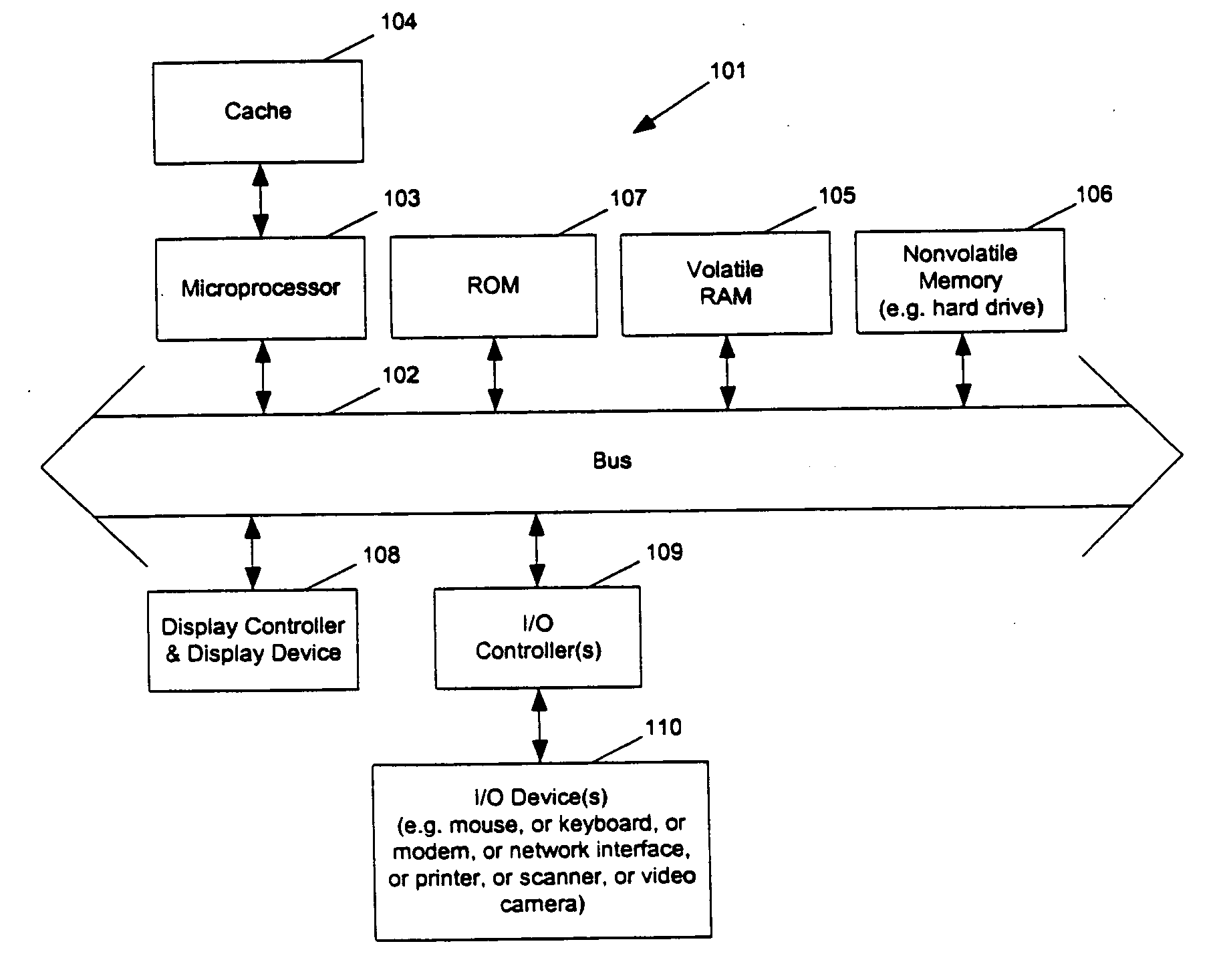
Figure 1 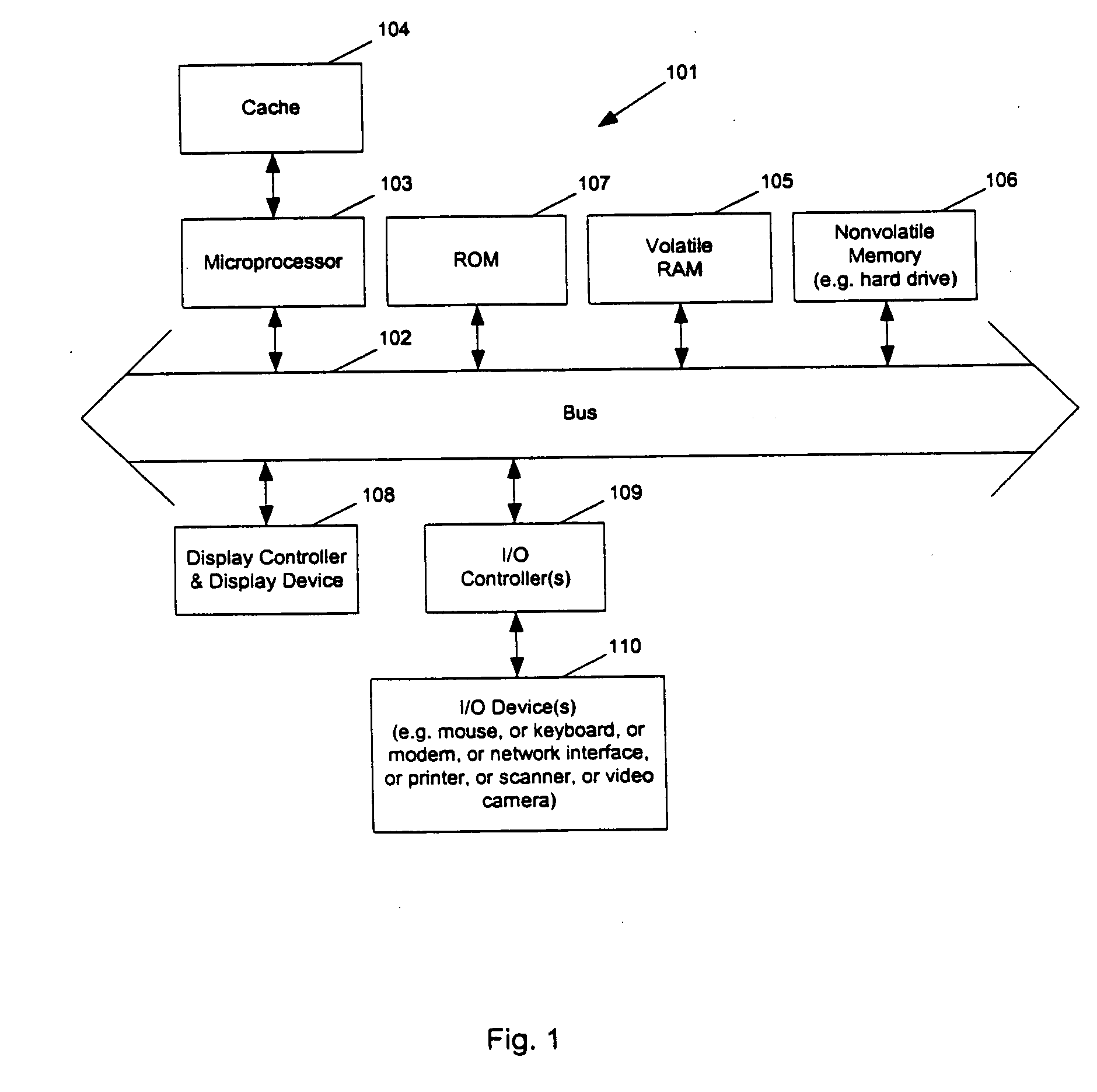
Figure 2 
Figure 3
Abstract
Description
[0001] This application is a continuation-in-part of U.S. patent application Ser. No. 10 / 626,031, filed Jul. 23, 2003, which is related to and claims the benefit of the filing date of U.S. provisional application Ser. No. 60 / 399,760, filed Jul. 29, 2002, and entitled “Method and Apparatus for Designing Integrated Circuit Devices with Shielding” by the inventor Kenneth S. McElvain.FIELD OF THE INVENTION
[0002] The invention relates to designing integrated circuits, and more particularly to shielding wires from capacitive and inductive coupling. BACKGROUND OF THE INVENTION
[0003] Integrated Circuits (ICs) are used in numerous applications, such as cellular phones, wristwatch cameras, and hand-held organizers, and others. As the commercial markets and consumer demands for smaller Integrated Circuits grow, IC size requirement trends continue towards a small form factor and lowered power consumption.
[0004] For the design of digital circuits on the scale of VLSI (very large scale integra...
Examples
Embodiment Construction
[0069] The following description and drawings are illustrative of the invention and are not to be construed as limiting the invention. Numerous specific details are described to provide a thorough understanding of the present invention. However, in certain instances, well known or conventional details are not described in order to avoid obscuring the description of the present invention.
[0070] Many of the methods of the present invention may be performed with a digital processing system, such as a conventional, general purpose computer system. Special purpose computers which are designed or programmed to perform only one function may also be used.
[0071]FIG. 1 shows one example of a typical computer system which may be used with the present invention. Note that while FIG. 1 illustrates various components of a computer system, it is not intended to represent any particular architecture or manner of interconnecting the components as such details are not germane to the present inventi...