
Method for Recovering an On-State Forward Voltage and, Shrinking Stacking Faults in Bipolar Semiconductor Devices, and the Bipolar Semiconductor Devices
a technology of stacking faults and forward voltages, applied in semiconductor devices, semiconductor/solid-state device details, instruments, etc., can solve the problems of lowering the properties of elements, various crystal defects, and various crystal defects during the production process
Patent Information
- Authority / Receiving Office
- US · United States
- Patent Type
- Applications(United States)
- Current Assignee / Owner
- Publication Date
- 2009-08-06
- Estimated Expiration
- Not applicable · inactive patent
Smart Images
Figure 1 
Figure 2 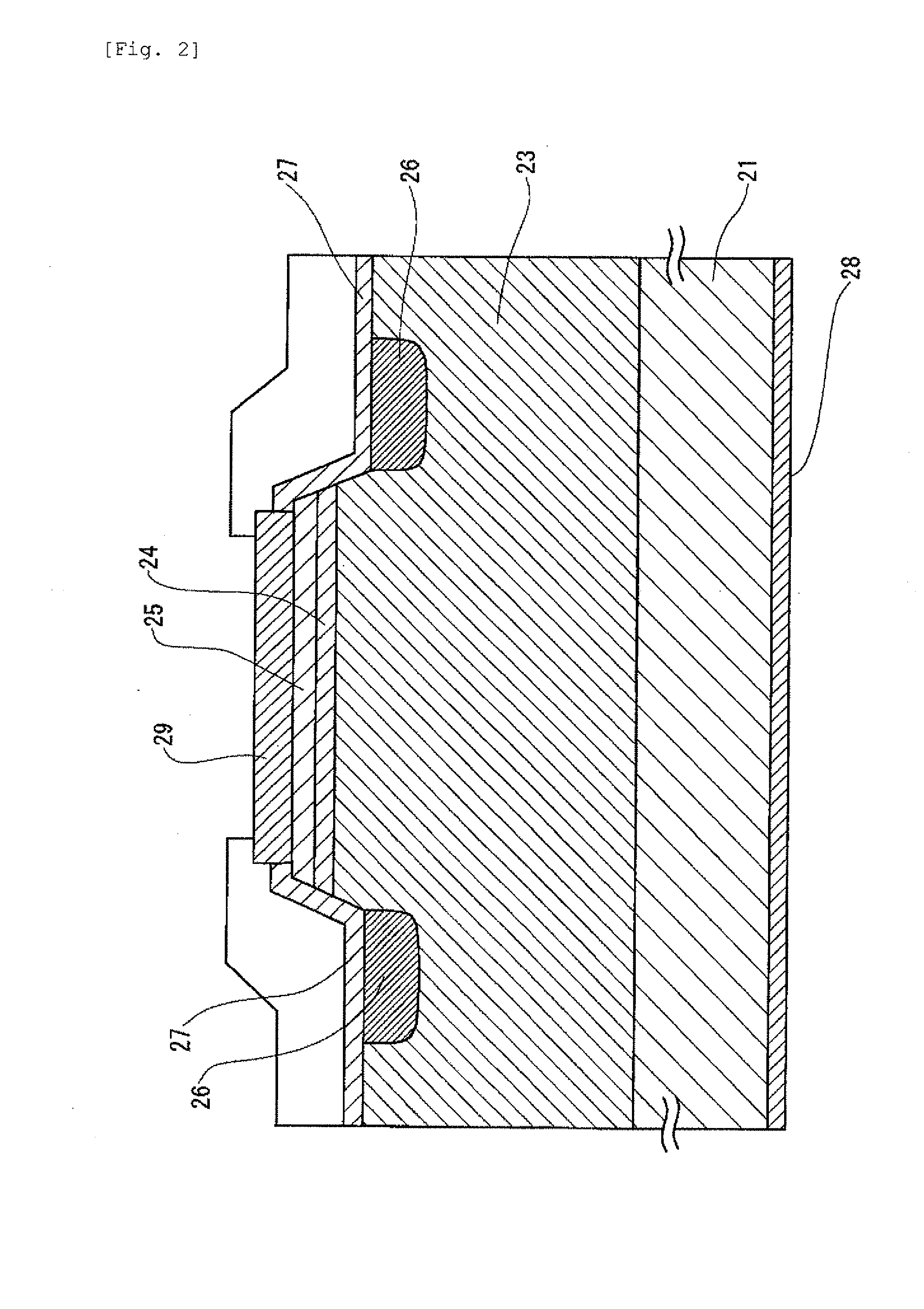
Figure 3
Abstract
Description
FIELD OF THE INVENTION
[0001] The present invention relates to a method for recovering an on-state forward voltage increased by on-state forward bias operation in a bipolar semiconductor device such that electrons and holes are recombined at the time of on-state forward bias operation in a silicon carbide epitaxial film grown on the surface of a silicon carbide single crystal substrate, a method for shrinking stacking faults which area has been enlarged by on-state forward bias operation, and a bipolar semiconductor device equipped with elements suitable for these methods.BACKGROUND OF THE INVENTION
[0002] Silicon carbide (SiC) is a semiconductor having a dielectric breakdown field intensity about ten times as much as that of silicon (Si), and further having excellent physical values on thermal conductivity, electron mobility and band gap. Accordingly, silicon carbide has been expected as a semiconductor material capable of improving capability of semiconductor elements greatly as compa...
Examples
example 1
[0118]A pn diode as shown in FIG. 2 was prepared for test. On an n type 4H-SiC (0001) substrate (carrier density of 8×1018 cm−3, 400 μm thick) prepared by slicing an ingot grown by the modified Lely method in an off direction of [11-20] at an off angle of 8° and mirror treating the surface, a nitrogen doped n type SiC layer (donor density of 5×1014 cm−3, 40 μm thick), and an aluminum doped p type SiC layer (p type junction layer: acceptor density of 5×1017 cm−3, 1.5 μm thick and p+ type contact layer: acceptor density of 1×1018 cm−3, 0.5 μm thick) were epitaxially grown in this order.
[0119]Next, the outer peripheral part of the epitaxial film was removed by reacting ion etching (RIE) and a mesa structure having a vertical width of 4 μm was formed. In order to ease the electric field concentration in the mesa bottom, aluminum ions were implanted to the mesa bottom and thereby a JTE having a total dose amount of 1.2×1013 cm−2, a width of 250 μm and a depth of 0.7 μm. After implantatio...
example 2
[0122]Using the pn diode same as prepared in Example 1, an on-state forward bias operation test was carried out in the same conditions as in Example 1. Successively, heating was carried out at 400° C. for 1 hr. Thereafter, the voltage in the forward direction was observed. The results are shown in FIG. 3.
example 3
[0123]Using the pn diode same as prepared in Example 1, an on-state forward bias operation test was carried out in the same conditions as in Example 1. Successively, heating was carried out at 500° C. for 1 hr. Thereafter, the voltage in the forward direction was observed. The results are shown in FIG. 3.