
Transparent substrate for optical elements, polarizer plate for liquid crystal display device using said substrate, and organic electroluminescence element
Patent Information
- Authority / Receiving Office
- US · United States
- Current Assignee / Owner
- Publication Date
- 2015-03-12
Smart Images
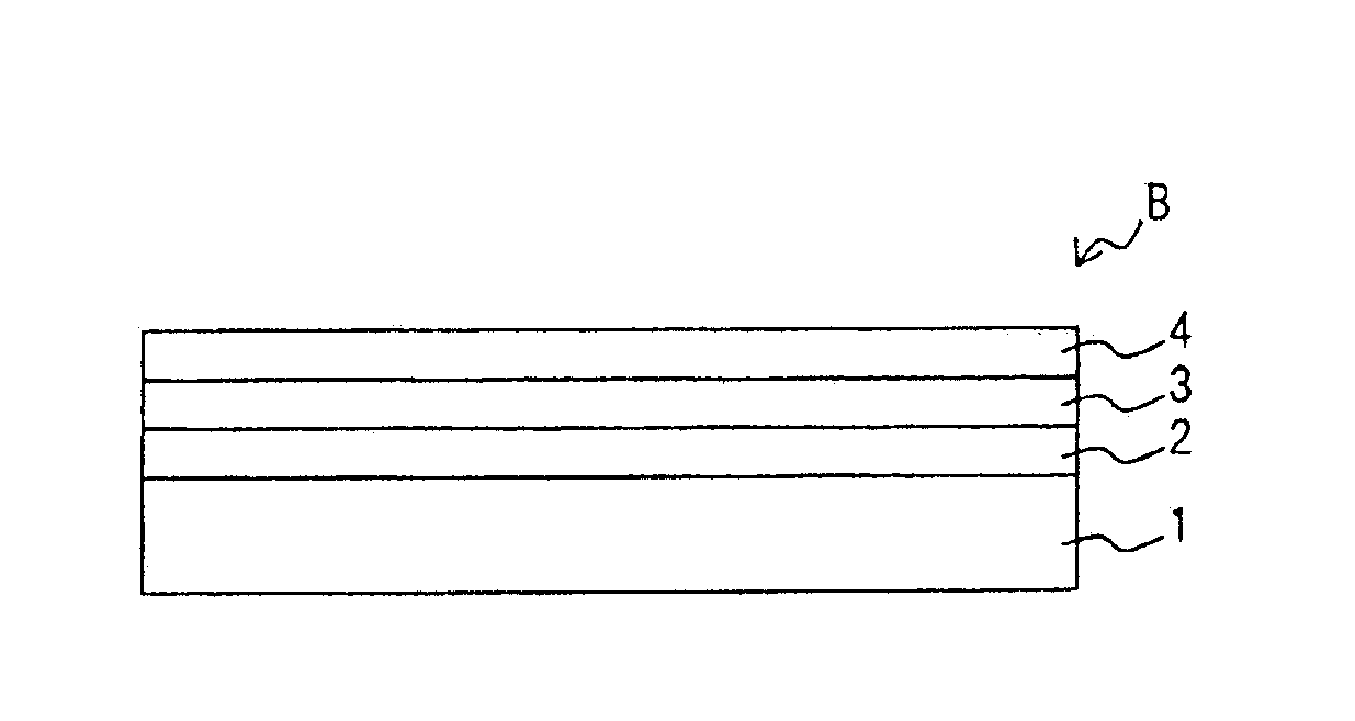
Figure 1 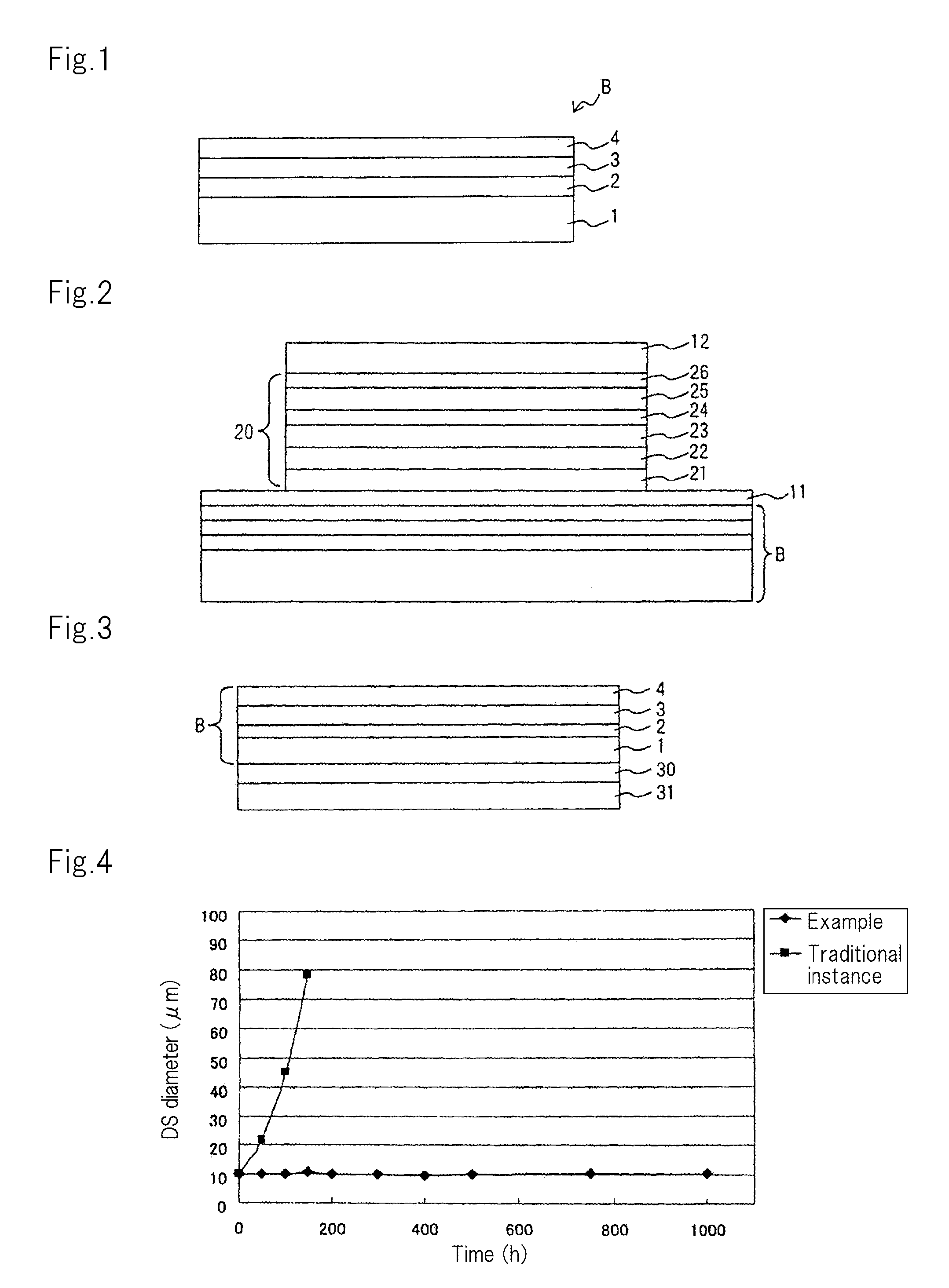
Figure 2 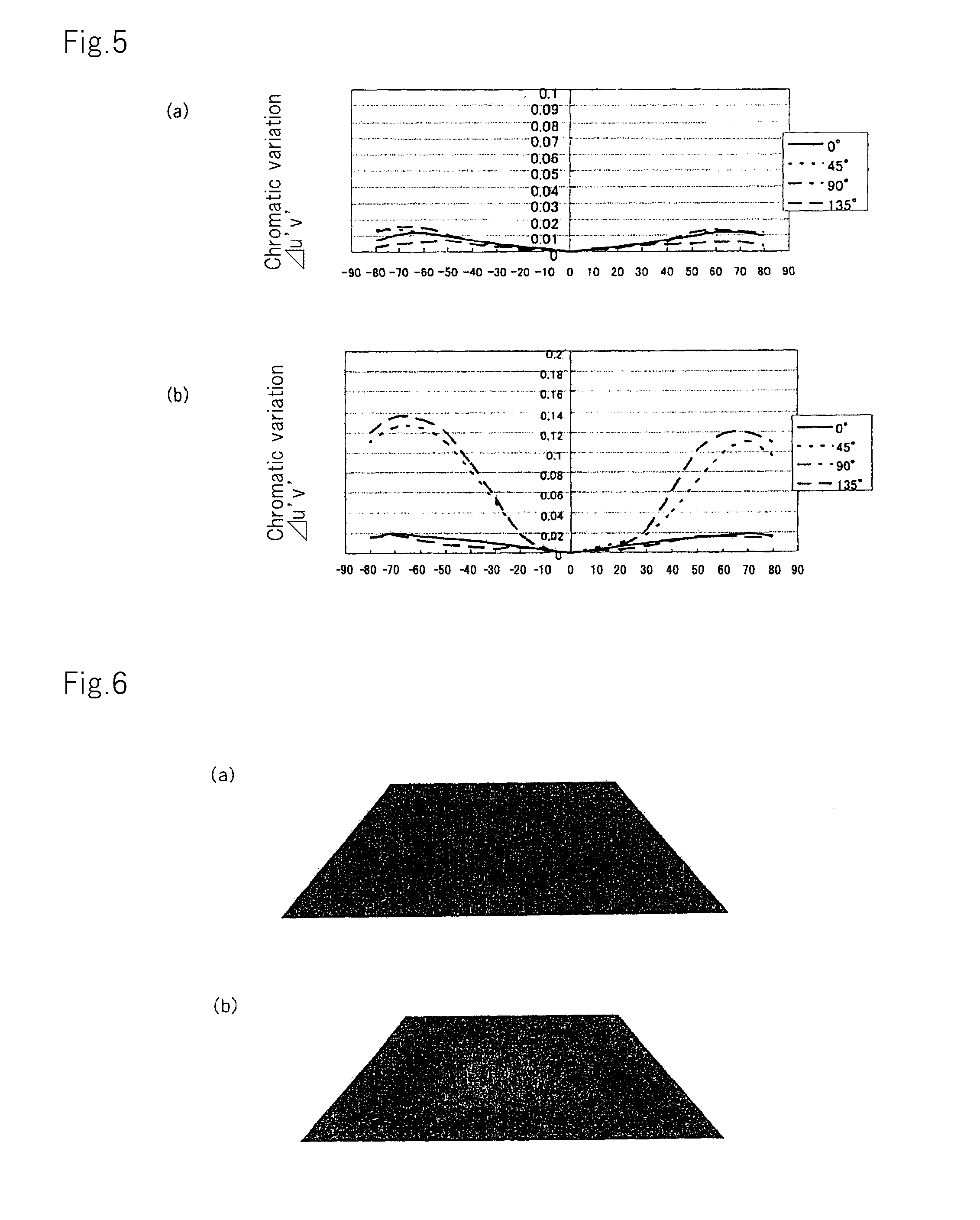
Figure 3
Abstract
Description
TECHNICAL FIELD
[0001] The present invention relates to a transparent substrate for optical elements, as well as a polarizer plate for a liquid crystal display device and an organic electroluminescence element.BACKGROUND
[0002] Since optical elements used in slimming devices such as organic electroluminescence (organic EL) illumination devices or liquid crystal display devices are required to have high light transmission, transparency and stiffness, a glass substrate is employed as a substrate for optical elements. However, such a glass substrate is fragile, as well as is not easy to manufacture and handle it. As more miniaturization, slimming, lightweight and further flexibility are required for such optical devices, a transparent and flexible resin film may be usefully used instead of a glass substrate because the resin film is capable of winding as a roll, is easy to handle, is efficiently manufactured, has an improved design properties, and is inexpensive.
[0003] Meanwhile, since resi...
Examples
example 1
[0083]A transparent substrate for optical elements was manufactured as follows: 100 nm thick polyethylenenaphthalate (TEONEX Q65FA; made by Teijin DuPont Films Japan Limited) was used as a flexible film (1), and a silicone nitride film layer (2), a hydrophilic layer (3) and a hydrophobic layer (4) were sequentially laminated on the flexible film (1). The silicone nitride film was formed as a transparent inorganic film having 100 nm thickness by introducing SiH4, NH3, H2 and N2 gases at flow rates of 10, 20, 200 and 200 sccm, respectively, at substrate temperature 100° C., internal pressure 120 Pa, power source frequency 13.56 MHz and input power 500 W using a plasma CVD device. Then, a hydrophilic layer was formed. A coating was performed by a spin coating method using methyl methacrylate as a monomer, propylene glycol monomethyl ether acetate as a solvent, a methacrylic ester monomer as a cross-linking agent, a modified polyacrylate as a dispersion-leveling agent, and a benzophenon...
example 2
[0089]A polarizer plate as shown in FIG. 3 was manufactured by bonding a transparent substrate for optical elements and a protective film (31) of 70 nm thick triacetyl cellulose film on both surfaces of a polarizer film (30) via 10 nm thick acrylic adhesive layer, respectively, wherein the transparent substrate for optical elements was made by the same method as in Example 1 except for changing the resin film to a 70 nm thick triacetyl cellulose film. The 70 nm thick triacetyl cellulose film was obtained by the following method. A solution of triacetyl cellulose in methylene chloride was uniformly coated on a flat substrate such as stainless, dried under reduced pressure at 47 kPa for 120 seconds, and further dried under heating at 50° C. for 5 minutes. Then, the resulting film was removed from the stainless plate and dried at 150° C. for 10 minutes without any stress on the film, thereby obtaining the 70 nm protective film.
[0090]Each of two polarizer plates was adhered to a color f...
example 3
[0095]As shown in FIG. 7, an inorganic layer was manufactured by the following method, in which a silicone nitride oxide film (first layer) (2a), a silicone nitride film (second layer) (second layer) (2b), a silicone oxide film (third layer) (2c) were sequentially laminated on a resin film (1). The silicone nitride oxide film was formed as a 70 nm thick transparent inorganic film using a plasma CVD device by introducing SiH4, O2 and N2 gases at the respective flow rates of 10, 20 and 200 sccm while maintaining 100° C. substrate temperature and 120Pa internal pressure at 13.56 MHz power supply frequency and 500 W input power. Then, the silicone nitride film was formed as a 100 nm thick transparent inorganic film by introducing SiH4, NH3, H2 and N2 gases at the respective flow rates of 10, 20, 200 and 200 sccm under the same condition. Further, the silicone oxide film was formed as a 100 nm thick transparent inorganic film by introducing SiH4, 02 and H2 gases at the respective flow ra...