
Multielement positional phase shift keying modulation and demodulation method
A technology of phase-shift keying and demodulation method, which is applied in the direction of phase-modulated carrier system, etc., can solve the problems of inconvenient high-ary modulation, etc., achieve the effect of flexible performance design and index adjustment, simple structure, and ease of design difficulty
- Summary
- Abstract
- Description
- Claims
- Application Information
AI Technical Summary
Problems solved by technology
Method used
Image

Examples
Embodiment
[0045] Embodiment: system parameter: get carrier frequency f c = 465kHz, N = 10, phase deflection Sampling rate f s =10f c = 4.65MHz, r g =0, then the carrier period T=1 / f c , symbol rate=1 / (10T)=46.5kHz.
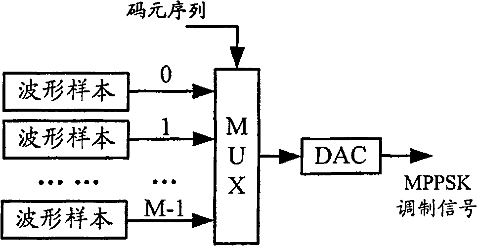
[0046] Such as figure 1 As shown, the sampling value of the basic waveform of the modulation symbol is stored in the waveform table, and the symbol value of the input symbol sequence is looked up in the table and the corresponding MPPSK modulated signal waveform is sent through the digital-to-analog converter (D / A). Using this hardware lookup table implementation, even if a non-zero guard interval r is inserted g , and will not add additional computation and overhead.
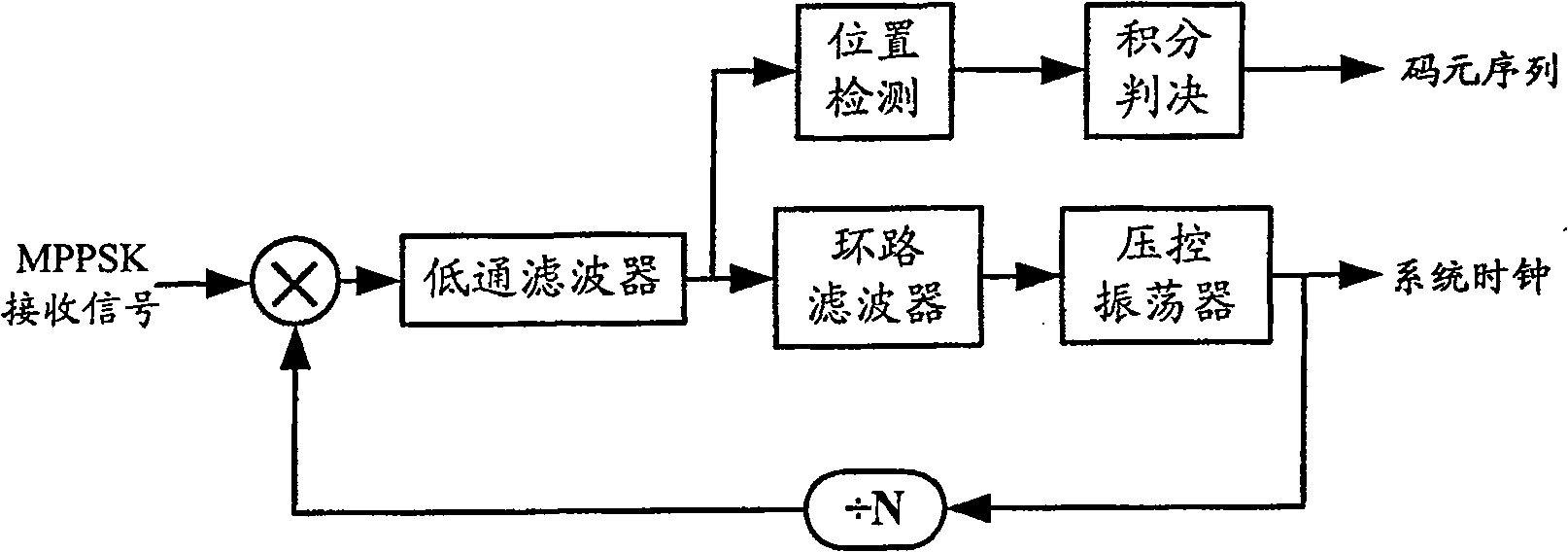
[0047] Such as figure 2 As shown, a signal demodulator structure based on a phase-locked loop is adopted. When carrier synchronization and symbol synchronization are realized, position detection and integral judgment are performed on the PD output to realize signal demodulation.
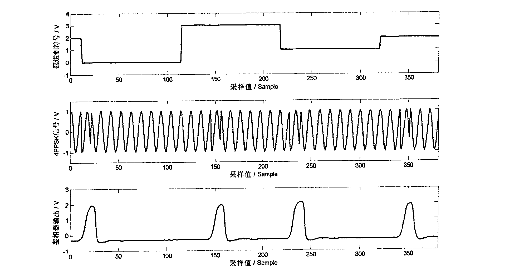
[0048] image 3...
PUM
 Abstract
Description
Claims
Application Information