Method and system for preparing high vacuum field modulation organic small molecular orientation nano film

A nano-film and preparation system technology, applied in vacuum evaporation plating, ion implantation plating, semiconductor/solid-state device manufacturing, etc.

Inactive Publication Date: 2009-06-24
BEIJING JIAOTONG UNIV
View PDF0 Cites 3 Cited by
  • Summary
  • Abstract
  • Description
  • Claims
  • Application Information

AI Technical Summary

Problems solved by technology

[0005] The preparation of oriented nano-films of small organic molecules modulated by the field i...

Method used


Image

  • Method and system for preparing high vacuum field modulation organic small molecular orientation nano film
  • Method and system for preparing high vacuum field modulation organic small molecular orientation nano film

Examples


Embodiment Construction

[0020] The present invention will be further described in conjunction with accompanying drawings.

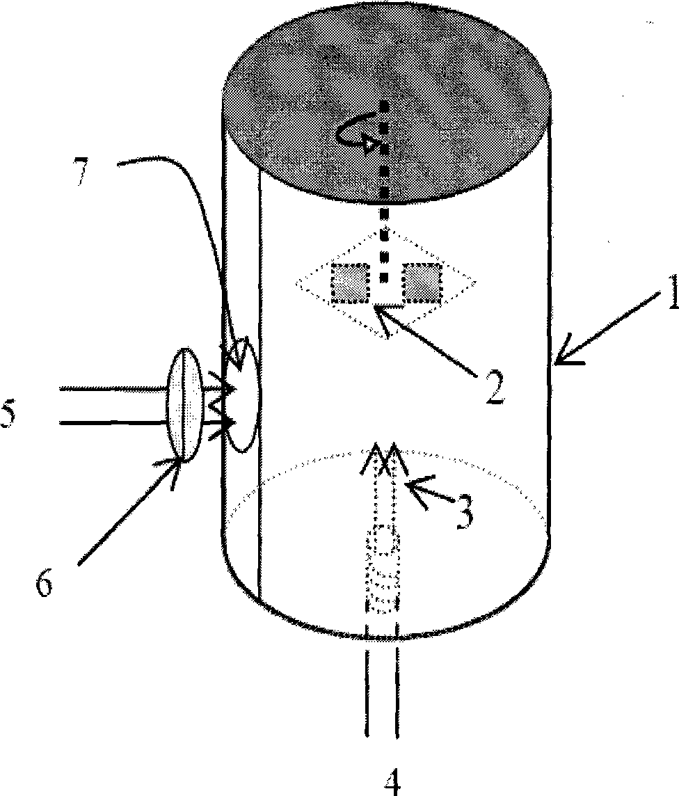
[0021] The preparation system of organic small molecule oriented nano-films modulated by high vacuum field, see figure 1 , it includes opening a glass window 7 with a diameter of 10 cm sealed with the cavity in the middle of one side of the high-vacuum evaporation chamber 1, and outside the high-vacuum evaporation chamber, a polarizer 6 that can be adjusted in a direction is fixed next to the glass window. A white light source 5 with adjustable light intensity is placed in front of the polarizer.

[0022] Preparation method 1 of organic small molecule oriented nano-film modulated by high vacuum field:

[0023] Deposition of octahydroxyquinoline aluminum (Alq 3 )A step of:

[0024] Step 1, give Alq 3 The evaporation boat 3 is connected to direct current, and the evaporation rate is 0.1nm / s;

[0025] Step 2, when evaporating, inject a beam of white light into the vacuum cavit...


PUM


Abstract

The invention discloses a method for preparing a high vacuum field modulation organic micromolecule oriented nano-film and a system thereof. The nano-film is applicable to all organic semiconductor devices. The method comprises the steps: an evaporation boat (3) filled with organic micromolecule materials is electrified with direct current, and the evaporation rate of the organic micromolecule materials is controlled within the range of 0.1nm/s-0.3nm/s; a beam of white light with the light intensity of 100-1000 candela is emitted into a vacuum cavity in an incident way, a beam of linearly polarized light having the light vector direction being parallel to evaporation particle flow is obtained through a polaroid sheet (6) arranged in front of a glass window (7), and the orientation of the single organic micromolecule is modulated by the polarized light; the organic micromolecule nano-film which is distributed in an oriented way is formed. The system is provided with the glass window which is sealed with the cavity and has the diameter of 10cm in the middle of one side of a high vacuum evaporation cavity (1); the polaroid sheet having the adjustable direction is fixed closely to the glass window, and a white light source (5) with adjustable light intensity is placed in front of the polaroid sheet.

Description

technical field [0001] The invention relates to a field modulation method and system based on an organic small molecule oriented nano film, and the organic nano film can be applied to all organic semiconductor devices. Background technique [0002] In 2000, the American "Science" magazine listed the progress of organic electronics as one of the top ten scientific and technological achievements in 2000, including major discoveries such as the draft human genome and cloning technology. In the same year, the Nobel Prize in Chemistry was awarded to Hegel, McDiarmid, Hideki Shirakawa and others for their major breakthroughs in organic electronics and organic / polymer research. Therefore, people have reason to believe that with the deepening of organic electronics research and the improvement of the preparation process of organic electronic devices, a new era - the era of organic electronics will come. [0003] Organic electronic materials and their application in the field of inf...

Claims


Application Information

Patent Timeline
IPC IPC(8): C23C14/12H01L51/00
Inventor 张福俊徐征王永生赵谡玲卢丽芳
Owner BEIJING JIAOTONG UNIV
Why Eureka
Try Eureka