
I/O (input/output)pin allotting method for nano CMOS (Complementary Metal-Oxide-Semiconductor Transistor) circuit structure
A technology of circuit structure and distribution method, applied in circuits, electrical components, electrical digital data processing, etc., can solve problems such as skyrocketing manufacturing costs, hindering signal integrity, and serious wiring crosstalk.
- Summary
- Abstract
- Description
- Claims
- Application Information
AI Technical Summary
Problems solved by technology
Method used
Image

Examples
Embodiment 1
[0039] Embodiment one: step 1.: define the circuit netlist and include I / O pin, logic gate unit and interconnection line, take as Figure 6 The netlist of the input circuit based on the NOR gate is shown, and the I pin and the O pin in the input circuit netlist are saved separately to the collection , in, then , , the total number of I / O pins is , save the logic gate units in the input circuit netlist to the set G, then , the number of logic gate units is ;
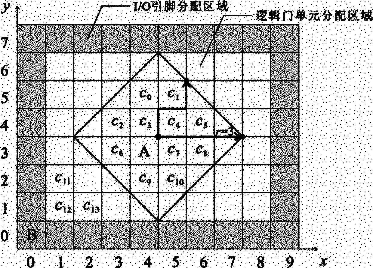
[0040] Step ②: Define the nano-CMOS circuit structure as a two-dimensional cell array , whose size is , the horizontal coordinates are , the vertical coordinate is ,in is a nano-CMOS unit, that is, the number of nano-CMOS units ; The outermost nano-CMOS unit of the two-dimensional cell array is an I / O pin allocation area, and the remaining nano-CMOS cells of the two-dimensional cell array are logic gate cell allocation areas; in the formula (2) is the redundant control parameter, The value is 2...
Embodiment 2
[0045] Step ①: Define the circuit netlist including I / O pins, logic gate units and interconnection lines, such as Figure 9 The netlist of the input circuit based on the NOR gate is shown, and the I pin and the O pin in the input circuit netlist are saved separately to the collection , in, then , , the total number of I / O pins is . Save the logic gate units in the input circuit netlist to the set G, , the number of logic gates is ;
[0046] Step ②: Define the nano-CMOS circuit structure as a two-dimensional cell array , whose size is , the horizontal coordinates are , the vertical coordinate is ,in is a nano-CMOS unit, that is, the number of nano-CMOS units ; The outermost nano-CMOS unit of the two-dimensional cell array is an I / O pin allocation area, and the remaining nano-CMOS cells of the two-dimensional cell array are logic gate cell allocation areas; in the formula (2) is the redundant control parameter, The value is 40; according to formulas ...
PUM
 Abstract
Description
Claims
Application Information