

touch panel
A technology of touch panels and substrates, applied in instruments, electrical digital data processing, input/output process of data processing, etc., can solve problems such as product damage, unreachable quality, poor flexibility, etc., and achieve high light penetration The effects of transmittance, low areal resistance, and good flexibility
Patent Information
- Authority / Receiving Office
- CN · China
- Current Assignee / Owner
- Publication Date
- 2011-12-28
- Estimated Expiration
- Not applicable · inactive patent
Smart Images
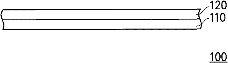
Figure 1 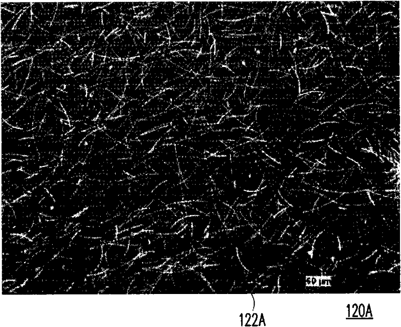
Figure 2 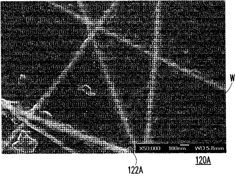
Figure 3
Abstract
Description
technical field
[0001] The invention relates to a touch panel, in particular to a touch panel with high light transmittance and low surface impedance. Background technique
[0002] In order to achieve more convenience, smaller size and more user-friendly, the input methods of many information products have changed from traditional keyboards or mice to touch-sensitive devices. The touch-sensitive device can be assembled on various types of flat-panel displays, so that the flat-panel displays can display images and input operation information.
[0003] As far as current common touch devices are concerned, capacitive touch panels and resistive touch panels are the most popular. In particular, users only need to lightly touch the surface of the capacitive touch panel to perform touch operations, which makes the capacitive touch panel more popular with users.
[0004] It is worth mentioning that no matter the capacitive touch panel or the resistive touch panel, a whole layer of...
Examples
Embodiment Construction
[0022] figure 1 It is a partial cross-sectional schematic diagram of the touch panel of the present invention. Please refer to figure 1 , the touch panel 100 includes a flexible substrate 110 and a conductive film 120 . The conductive film 120 is disposed on the flexible substrate 110 . In this embodiment, in order to make the touch panel 100 have good light penetration properties and good sensing accuracy, the areal resistance of the conductive film 120 must be between 10 -4 ohm / square to 200 ohm / square, and the light transmittance of the conductive film 120 is at least 87%. That is to say, the conductive film 120 of the present invention must have both high light transmittance and low surface resistance so that the touch panel 100 has ideal quality.
[0023] In order to realize the characteristics of light transmittance and low surface resistance, the following description will specifically propose implementations of a plurality of conductive films, but the following imp...