Timer device comprising advanced reduced instruction set computer machine (ARM) and field programmable gate array (FPGA) and implementation method thereof

A timer and timing technology, which is applied to program control and electrical program control in sequence/logic controllers, can solve the problems of execution speed influence, large circuit scale, and heavy maintenance workload, etc.

Inactive Publication Date: 2012-01-18
GUANGXI UNIVERSITY OF TECHNOLOGY
View PDF5 Cites 17 Cited by
  • Summary
  • Abstract
  • Description
  • Claims
  • Application Information

AI Technical Summary

Problems solved by technology

[0004] 2. Applying the timing interrupt method of the reference timer, the CPU responds and exits the reference timer interrupt service program to occupy the CPU running time; although the query method of the fourth method does not need to respond and exit the interrupt operation, the system program needs to query and exit once. Judgment once; the smaller the timing reference time, such as 1ms, the more timers in the timer system, the longer the CPU will be occupied, which will have a serious impact on the execution speed of other program modules, and the timing accuracy is not high;
[0006] The fifth method is to use non-programmable hardware timing, and each timer is realized by an independent hardware circuit; in this way to realize the timing function, the more timers are required, the larger the circuit scale and the maintenance workload is.

Method used


Image

  • Timer device comprising advanced reduced instruction set computer machine (ARM) and field programmable gate array (FPGA) and implementation method thereof
  • Timer device comprising advanced reduced instruction set computer machine (ARM) and field programmable gate array (FPGA) and implementation method thereof
  • Timer device comprising advanced reduced instruction set computer machine (ARM) and field programmable gate array (FPGA) and implementation method thereof

Examples


Embodiment 1

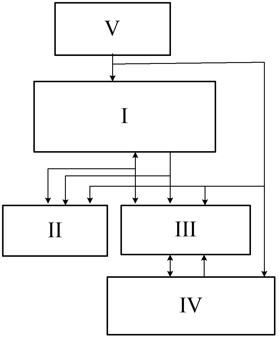
[0145] A timer device composed of ARM+FPGA, such as figure 1 As shown, the timer device includes ARM control module Ⅰ, memory module Ⅱ, FPGA timer module Ⅳ, dual-port RAM module Ⅲ and power supply module Ⅴ; ARM control module Ⅰ is connected with memory module Ⅱ and dual-port RAM module Ⅲ respectively , the FPGA timer module IV is connected to the dual-port RAM module III, and the power module V converts the external power supply into a voltage that meets the requirements through the voltage circuit, which is ARM control module I, memory module II, dual-port RAM module III and FPGA timer module ⅣProvide transformed DC power supply;

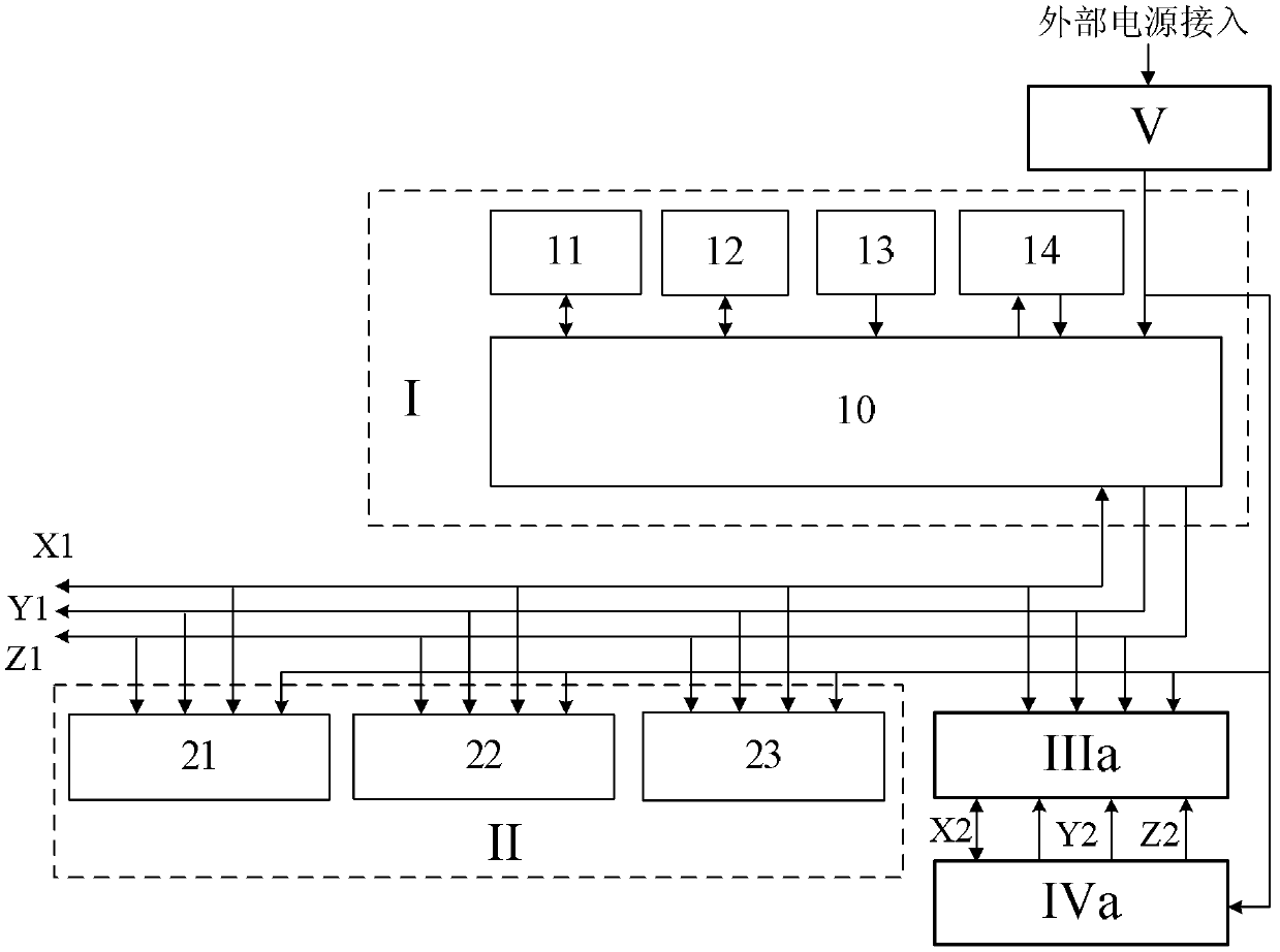
[0146] Such as figure 2 As shown, the ARM control module I includes an embedded ARM microprocessor 10, a human-computer interaction circuit 11, a control circuit 12, a reset circuit 13, and a JTAG debugging interface circuit 14, and the embedded ARM microprocessor 10 is used as the control core, respectively Connect with human-computer interacti...

Embodiment 2

[0160] A timer device composed of ARM+FPGA, its basic structure is the same as that of Embodiment 1, and also uses the embedded ARM microprocessor as the control module, FPGA as the timing processing module, including ARM control module I, memory module II, FPGA timing Module IV, dual-port RAM module III and power module V; ARM control module I is connected to memory module II and dual-port RAM module III respectively, FPGA timer module IV is connected to dual-port RAM module III, and power module V is ARM control Module Ⅰ, memory module Ⅱ, dual-port RAM module Ⅲ and FPGA timer module Ⅳ provide power supply; The difference between the present embodiment 2 and embodiment 1 is: in embodiment 1, dual-port RAM module Ⅲ and the timing timer composed of FPGA1 The device module IV is two independent modules; and in the present embodiment, the dual-port RAM module III is embedded in the FPGA2 forming the FPGA timer module IV, and FPGA2 is a block with the dual-port RAM module III and t...

Embodiment 3

[0162] The method for implementing the timer by using the timer device composed of the above-mentioned ARM+FPGA is to use the embedded ARM microprocessor in the ARM control module as the control core, to carry out timing control processing with the FPGA timer module, and to use the dual-port RAM module as the control core. The bridge for data transmission between the ARM control module and the FPGA timer module to realize data communication; during the initialization process of the embedded ARM microprocessor, clear each storage unit of the dual-port RAM and clear the timing unit in the FPGA ;

[0163] In the process of compiling the user program, the ARM control module transmits the timing parameters and usage status information set by each numbered timer used by the user program to the dual-port RAM module, and the ARM control module executes the timer of a certain numbered timer in the user program. When outputting, the running state information of the numbered timer is tra...


PUM


Abstract

The invention relates to a timer device comprising an advanced reduced instruction set computer machine (ARM) and a field programmable gate array (FPGA), which is characterized by taking an embedded ARM microprocessor as a control module and the FPGA as a timing processing module, and comprises an ARM control module, a memory module, an FPGA timer module, a two-port random access memory (RAM) module and a power module, wherein the ARM control module is respectively connected with the memory module and the two-port RAM module; the FPGA timer module is connected with the two-port RAM module; when a large-scale time control program or a programmable controller user program is executed by the ARM control module, under the condition that a timer meets the running requirement, running state information is transmitted to the two-port RAM module by the ARM control module; under the condition that the timer does not meet the running requirement, running stopping information is transmitted tothe two-port RAM module; and when soft contact storage unit information is read by the program, contact state information is read from the two-port RAM module by the ARM control module. By adopting the device and the method for realizing the timer thereof, the timing precision is high, and the execution time of the PLC user program is not occupied.

Description

technical field [0001] The present invention relates to a timer device and a timing method, in particular to a timer device for a large-scale time control device or a programmable logic controller (PLC) and an implementation method thereof. Background technique [0002] In the application system of large-scale time control or programmable logic controller (PLC), a large number of timers will be used, and there are usually five ways to realize them: the first and second ways are the application of a timer in the microprocessor. The timing time is used as the reference time, and the timing parameters of each timer are stored in a storage unit, and the timer interrupt method is used for programming. There are two main programming methods. The first method is to program the timer judgment in the reference timer interrupt service program. Processing program, the reference timer regularly sends interrupt signals according to the reference time. In the reference timer interrupt ser...

Claims


Application Information

Patent Timeline
Patent Type & Authority Applications(China)
IPC IPC(8): G05B19/05
Inventor 李克俭蔡启仲潘绍明付杰吴笔迅
Owner GUANGXI UNIVERSITY OF TECHNOLOGY
Why Eureka
Try Eureka