Liquid crystal display device
一种液晶显示装置、液晶层的技术,应用在静态指示器、非线性光学、仪器等方向,能够解决显示不均匀等问题
- Summary
- Abstract
- Description
- Claims
- Application Information
AI Technical Summary
Problems solved by technology
Method used
Image

Examples
Embodiment 1
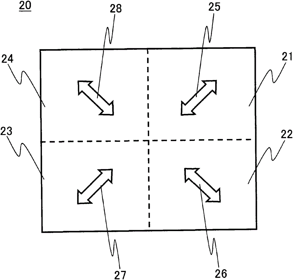
[0143] The liquid crystal display device of Example 1 was produced by applying the above-mentioned liquid crystal 2 to the vertical alignment type liquid crystal display device capable of multi-channel driving in the present embodiment. Set the electrode structure of the pixel of the liquid crystal display device of embodiment 1 and Figure 10 The above-described first example of the second electrode form applicable to the vertical alignment type liquid crystal display device of this embodiment is the same. In this case, the size of one pixel was set to 0.39 mm square, the formation pitch of the sub-pixels was set to 80 μm, and the width of each linear cutout was set to 10 μm. The panel resistivity is 4.6×10 10 Ω cm. It is known that using the vertical alignment type liquid crystal display device of Example 1, the time from when static electricity is applied to the substrate surface of the display liquid crystal layer to when the charge is eliminated is 5 seconds, which is a...
Embodiment 2
[0146] The above-mentioned liquid crystal 2 was applied to the vertical alignment type liquid crystal display device capable of multi-channel driving in the above-mentioned embodiment to manufacture the liquid crystal display device of Example 2. Set the electrode structure of the pixel of the liquid crystal display device of embodiment 2 and Figure 6 The above-described first example of the first electrode form applicable to the vertical alignment type liquid crystal display device of this embodiment is the same. In this case, the size of one pixel was set to 0.39 mm square, the formation pitch of the sub-pixels was set to 80 μm, and the width of the linearly extending slit portion of the curved slit was set to 10 μm. The panel resistivity is 4.6×10 10 Ω cm.
[0147] It is known that using the vertical alignment type liquid crystal display device of Example 2, the time from the application of static electricity to the substrate surface of the display liquid crystal layer t...
Embodiment 3
[0150] The liquid crystal display device of Example 3 was manufactured by applying the liquid crystal 2 described above to the vertical alignment type liquid crystal display device capable of multi-channel driving in the present embodiment. Set the electrode structure of the pixel of the liquid crystal display device of embodiment 3 and Figure 11 The above-described second example of the second electrode form applicable to the vertical alignment type liquid crystal display device of this embodiment is the same. In this case, the size of one pixel was set to 0.39 mm square, the formation pitch of the sub-pixels was set to 80 μm, and the width of each linear cutout was set to 10 μm. The panel resistivity is 4.6×10 10 Ω cm. It is known that using the vertical alignment type liquid crystal display device of Example 3, the time from the application of static electricity to the substrate surface of the display liquid crystal layer to the elimination of the charge is 5 seconds, wh...
PUM
| Property | Measurement | Unit |
|---|---|---|
| size | aaaaa | aaaaa |
| size | aaaaa | aaaaa |
Abstract
Description
Claims
Application Information
 - R&D
- Intellectual Property
- Life Sciences
- Materials
- Tech Scout
- Unparalleled Data Quality
- Higher Quality Content
- 60% Fewer Hallucinations
Browse by: Latest US Patents, China's latest patents, Technical Efficacy Thesaurus, Application Domain, Technology Topic, Popular Technical Reports.
© 2025 PatSnap. All rights reserved.Legal|Privacy policy|Modern Slavery Act Transparency Statement|Sitemap|About US| Contact US: help@patsnap.com